Replacing State Machine with Control Processor in an SoC Design Reduces Risk and Greatly Increases Design Flexibility
The Defense Advanced Research Projects Agency (DARPA) recently set a goal to design a 200-million transistor chip in 30 weeks with a 10-person team. DARPA expects to achieve this result through “increased reuse and lowered level of manpower and design expertise required to design and verify integrated circuits in leading-edge CMOS technology…“ according to the PDF at DARPA site*, Design reuse is the mainstay of SoCs going into consumer devices, automotive electronics, communications, and data center applications. It involves large collections of third party IP, applications processors, GPUs, DSPs, and more tied together by a high-speed on-chip bus fabric.
In addition to the computing resources, these SoCs also require memory controllers and any number of peripherals—PCI Express, NVM Express, MIPI, HDMI, SPI, PVT (process, voltage, temperature sensors), among others. Each of these elements comes with control signals such as error messages, status updates, etc. that need to be connected to logic or a stage machine to perform some function. In SoCs with multiple special processors all running independently and communicating with one another, monitoring their operation is even more difficult. Significant glue logic and state machines stitch together these many third party blocks into the larger design, creating significant design and verification overhead.
This glue logic and state machines have significant drawbacks. Foremost is the time and effort expended developing something that is not an integral part of the value-add of the final chip.
Next, any error or oversight in these circuits could cause a costly design spin and deployment risk. Finally, designing all of this in hardware significantly restricts the ability to make changes post-silicon. For example, something as simple as the boot sequence of when to power-up the various processors in the design is permanently fixed in a state machine. Any change in this sequence post silicon requires a design spin. These problems can be resolved if instead of glue logic and state machines, a system control processor is designed into the SoC to provide a form of SoC control intelligence—a personal assistant for all the elements on the SoC.
Value of a System Control Processor
The system control processor can execute functions in software that would otherwise be done by hardware logic. This is accomplished by connecting all the signals from third party IP blocks that are not directing the flow of data to and from the main applications processor to an on-chip microcontroller and writing software to manage these signals—buffer overflow, crc error, etc.
Having a system control processor to handle the status and control signals that are not required for the flow of data through peripherals and interfaces of the SoC design, total performance of the application process can be improved.
What are the benefits of this solution? The most compelling benefit is that software provides the design team the “do over” benefit, without requiring a hardware spin. Another benefit comes from adding intelligence to the operating control of the chip. Transferring all the status and control functions not essential to the main mission of the applications processor to a system control processor can help save power while improving the performance of the system. Another example is the boot sequence. If after the chip is fabricated the sequence needs to be altered it can be done with a simple software change. Managing power is another real benefit. PC vendors often update their BIOS to improve power management. A system control processor can offer the same flexibility at the SOC level. Rules for powering down or shutting off elements can be changed to improve system performance post silicon.
A Complete Platform for System Control
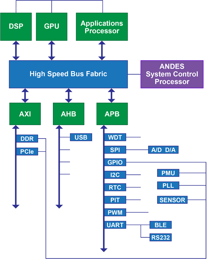
Incorporating a system control processor into a larger SoC design still requires integrating the memory and peripherals commonly found on all processors. Andes Technology Corporation has developed a platform for system control to reduce the effort of assembling these elements and the platform provides a more complete solution for SoC designers wanting to adopt the system control processor solution. The platform includes a system control processor core to monitor and control the operation of the SoC (see Figure) and the peripherals and bus fabric required by a typical SoC design. A complete software development package with demo examples is included to jump-start the programming of the embedded processor.
The bus fabric is an important part of platform, since it provides the ready-made communication link between the major compute engines of the SoC and its memory and peripherals elements. The bus fabric supplied in the platform is optimized for ease of use while being cost competitive.
It has an AXI, AHB, and APB fabric with configurable numbers of masters and slaves. In addition to the bus fabric and the Andes system control processor, the platform comes with a set of peripherals to provide the most common functions in a typical SoC design: SRAM bridge, GPIO, SPI, watchdog timer, programmable interval timer, and UART. Designers are freed from integrating these essential functions so they can concentrate on their value added design.
For designers wanting to reduce their design and silicon re-spin risk while enabling greater design flexibility once a design is in silicon, the Andes platform for system control provides a cost-effective solution. The platform comes fully assembled with software modules pre-packaged. Incorporating additional elements is a straightforward addition to the design and the creation of software code to interpret the sensor reading and act on the findings. And software development can be done in C code, making changes before and after silicon a simple program change, thus reducing risk and enhancing design flexibility.
Andes Custom Extension™ (ACE) Enables Customers to Add Application-Specific Instructions to AndesCore™ Processors
The exponential growth of smart device markets such as IoT and home automation appliances requires SoC designs to deliver high performance at minimum cost and low power consumption. To help designers address the challenge, the Andes Custom Extension™ (ACE) is invented for customers to add their own instructions to AndesCore™ processors. By combining highly performance efficient baseline features of AndesCore™ with the ACE instructions tailored for customers’ applications, SoCs can get the benefits from both sides: the complete flexibility of processor programmability and the absolute efficiency of hardwired engine.
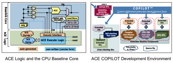
Users define ACE instruction first by profiling their C programs on Andes ISS simulator to identify the code segments which contribute to significant percentage of execution time. Those code segments then can become part of the instruction semantics in an ACE description file. The file also specifies the instruction mnemonic, the operand(s) and the estimated amount of cycle(s) to execute in hardware. Substituting the original code with ACE intrinsic functions which are automatically generated to represent the corresponding ACE assembly instructions, the application software can be profiled again to get the estimated performance improvements. If the results are satisfiable, user can go ahead to design the Verilog RTL representing the same functionality as the instructions. The Verilog is in a concise format which consists of only the execution logic while the manual work for connections to the CPU pipeline are not required. The ACE description file and concise Verilog file are all that customers need to design for ACE’s development environment.
The Custom-OPtimized Instruction deveLOpment Tools (COPILOT™) parses ACE description file and generates the shared libraries needed for the toolchain to recognize ACE instructions. It also parses the concise Verilog RTL and generates the complete extended ACE Verilog module to connect to the CPU pipeline. Then a new processor equipped with custom instructions is ready for SoC integration and software development. The simplicity of ACE and COPILOT™ environment allows user to focus on ACE instruction’s functionality itself without worrying about housekeeping functionality in the CPU pipeline. In addition, using the extended toolchain is the same as standard tools. Since the extended components are all generated locally, the light-weight flow lets users easily try out as many experiments as they need.
Deblocking filter is a computation intensive function used for improving visual quality by eliminating the blocking artifact introduced during video encoding. It can be optimized by defining the ACE instructions that implements data manipulation functions for performance, and leaving the control tasks in the software for flexibility. The performance, power and area (PPA) benchmark shows stunning results as ACE boosts performance by running 102 times faster, but consumes only 1/74 of the power.
ACE descriptions in C and Verilog enable high level behaviors to be implemented in a single instruction. For example by encapsulating hardware operators with loop semantics, ACE instructions can repeat their operations for a variable iteration count by itself. This is possible because ACE allows instructions to be single or multi cycles, fixed or variable cycles. With this high level construct, the repeated instruction fetches and decodes are eliminated. Therefore both performance and power consumption are greatly improved.
In addition to performance, power and cost, security for the software IP is another major concern for designers of intelligent devices. By converting C code segments into ACE instructions, design’s proprietary functionalities are concealed in hardware so that reverse engineering the program code will not reveal that information. Furthermore, since the ACE design flow is conducted completely within users’ computer, not required to be submitted over Internet to vendor’s server, the confidentiality of the design can be secured.
Andes Technology Corporation offer customers the instruction extension capability with the belief that every design is unique, and by enabling them to accelerate their own application-specific functions on the general-purpose processors, their applications will run more efficiently, and their products will be more competitive. On the contrary, some processor vendors keep tight control of their instruction set and do not allow users’ own addition, eventually it will be at their customers’ expense to migrate to higher performance cores.
Today’s SoC designers are confronted with the challenges to catch up with the dynamics of process technology advancements, industry standard revisions, fierce market competitions, and more. ACE brings programmable acceleration to SoC designs by boosting performance and power efficiency while maintaining programmability. It allows users to focus on the design rather than on the tools, to implement high-level functions as instructions, and above all, to protect software IP by hardware encapsulation. All those benefits offered by ACE together assist SoC designers to conquer the challenges of ever increasing complexity in today’s embedded systems.
Andes SaG Application Examples
Memory mapping is essential to embedded system software design and often implemented in linker scripts. However, many programmers find linker scripts difficult to write and maintain due to its complicated syntax and long descriptions. For those who develop projects based on AndesCore™, they find Andes SaG is a boon to replace linker scripts with simple and intuitive descriptive language. More and more developers reveal their preference for Andes SaG over linker scripts when providing feedbacks to Andes.
Having a technical article introducing and explaining SaG syntax before, in this article we center on four SaG application examples in an attempt to help developers better understand Andes SaG and provide them references during development.
1. Place a function or variable at a fixed address
The first example shows how to locate a function or variable at a fixed address – the address used here is a virtual address (VMA). There are a number of reasons for doing this. One is when the process address space of your SoC is not continuous and one is when you need to access high-efficient memory effectively. You have two steps: first, add your own defined section in a SaG file and specify its VMA to a fixed address; next, in your C code, specify functions or variables that are about to change to the section defined in the last step.
Figure 1 below demonstrates the first step. The key word “USER_SECTIONS” in line 1 denotes the following sections are all user-defined.
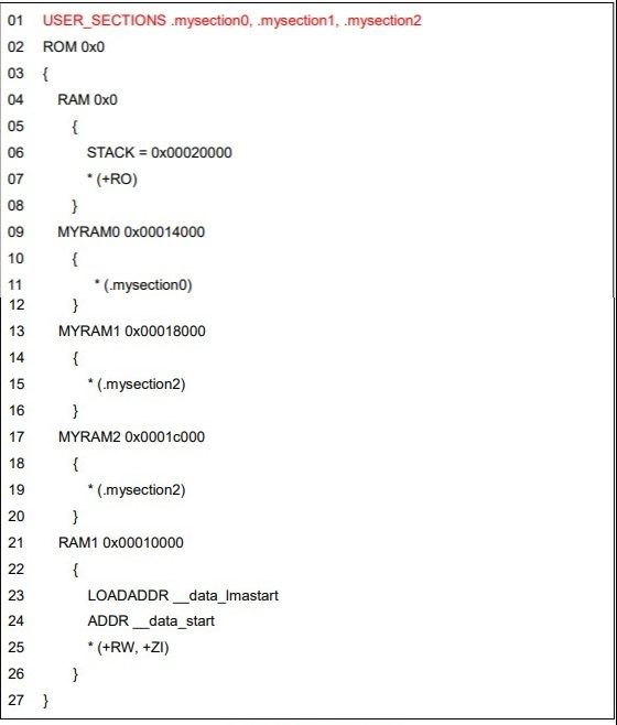
Figure 1. Samp1.sag
In Figure 1, line 4 to 8 show the memory region beginning from 0x0 is read-only and contains program codes (.text section) and read-only data (.rodata section). From line 9 to 12, the MYRAM0 part shows the VMA of .mysection0 begins from 0x00014000. Similarly, MYRAM1 and MYRAM2 parts present the beginning of VMA for .mysection1 and .mysection2 respectively. RAM1 in line 21 contains .data and .bss sections and its VMA begins with 0x00010000. That is, you should copy the data section from the load address (LMA) to the VMA in your C code and use data_lmastart and data_start to assign address values.
To specify functions to your own defined section, say, .mysection0, you have to use attribute ((section(“.mysection0”))) in your C code. Please refer to Figure 2A for the complete statement and Figure 2B for an alternative.
 Figure 2A. Specify a function to a user-defined section in C code
 Figure 2B. Another way to specify a function to a user-defined section
To specify a global variable, gdata1, to a user-defined section , .mysection1,define attribute ((section(“.mysection1”))) in your C code. Figure 3 below shows the complete statement.
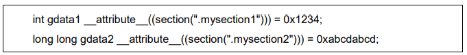 Figure 3. Specify a variable to a user-defined section
With functions and variables specified to fixed addresses like above, the ELF file generated after compilation reveals the VMA and LMA of each user-defined section, as shown in Figure 4.
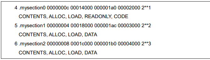 Figure 4. ELF Header
2. Change IVB at run time
You may want to execute separate ISR for the same interrupt at boot time and at run time. There are several ways to achieve this. The one introduced here is to implement a vector table that contains the entry of desired ISR and then use a SaG file to specify the vector table to a fixed address. That way, if you like to switch ISR after the boot time, you only have to modify the register IVBASE (ir3).
Thus, the key is to build a vector table in assembly code and assign it to a user-defined section. See Figure 5 for how it is implemented:
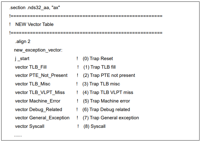 Figure 5. Specify a vector table to a user defined section
The point of Figure 5 lies on the first line where “.section” is used to define a non-standard section “.nds32_aa”. While Andes standard vector table is usually placed in the nds32_init section, the newly-created vector table is placed in .nds32_aa. As for “ax”, “a” denotes “allocable” and “x” means “executable”. Next, use a SaG file to specify the VMA of .nds32_aa to a fixed address, as shown in Figure 6 below:
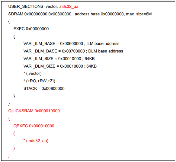 Figure 6. Specify the VMA of the user-defined section to a fixed address
Figure 6 shows that the first address of the new vector table is 0x10000 – this is the address you need to direct IVBASE to upon completion of the boot up process. That way, whenever an interrupt comes in, it will be led to the new vector table.
3. Specify sections of .o or .a files to a fixed address
The above two examples have something in common: both specify some part of the program to a user-defined section. They have something different too: in the first example, a C function or variable is assigned to a user-defined section; in the second example, an assembly function is assigned. Both cases involve modifications on source code. However, for some application scenarios that there is no source code but object files or static library like .o or .a, can you specify sections of these files to a fixed address as well? Please reference Figure 7A below. It exemplifies how to specify the VMA of an object file’s (hello.o’s) read-only segments, including program code (.text section) and read-only data (.rodata section), to a fixed address (0x10000 in this case).
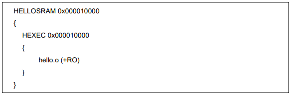 Figure 7A. Specify sections of an .o file to a fixed address
Though you can follow Figure 7A to list every .o file in your SaG file, it is not recommended for the SaG file will become difficult to read and maintain. A better solution is to exclude certain .o files with a directive like “EXCLUDE_FILE” in GNU linker script. Andes SaG also supports excluding files. Figure 7B demonstrates how to specify all sections of *uart.o files to a fixed address and in the meanwhile keep other files unchanged. As there is inconsistency between the LMA and VMA of *uart.o sections, the assignment in Figure 7B copies these sections from the LMA to VMA to resolve the problem.
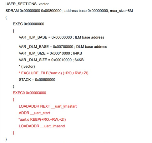
Figure 7B. Andes SaG supports “EXCLUDE_FILE”
4. Fix inconsistency between LMA and VMA
The first three examples show how to locate the VMA of some program section at a fixed address, which is also the basic function of linker scripts. When the LMA and VMA of a section are not equal, embedded software engineers need to copy the section from the LMA to VMA during program initialization. Both the LMA and VMA are assigned to specific values in the linker script for C code to reference.
Andes SaG also can assign specific values to variables LMA and VMA. Instead of close arrangement, there is alignment constraint on data storage. For example, the first address at which a 4-byte word stored needs to be 4-byte aligned; a program with specific optimization flags, such as -O3 using Andes compiler, also requires the first address of its functions to be 4-byte aligned. For gaps between sections resulting from such an alignment constraint, Andes SaG normally can handle them well. However, in some sophisticated cases, you’ll need to give Andes SaG more instructions to ensure it works properly.
Take Figure 7B as an example, the keyword “NEXT” in the statement “LOADADDR NEXT uart_lmastart” is used to notify SaG that the value of this variable must be gained from the beginning of the next section rather than the end of the last section. To make it clear, let’s look at Figure 8, the ELF file header generated after project compilation with the SaG file in Figure 7B:
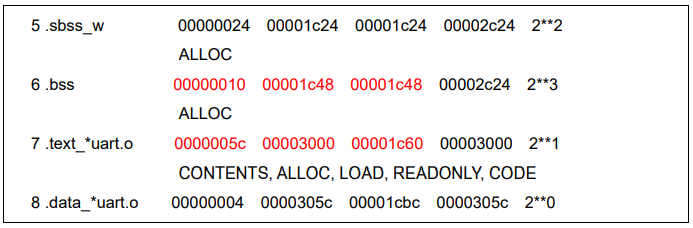 Figure 8. ELF header
Figure 8 shows the LMA of “.text_*uart.o” is 0x1c60. Namely, the LMA of the last section (.bss) must end at 0x1c48+0x10=0x1c58, which echoes the usage of “NEXT” in Figure 7B. The keyword explicitly indicates that “ uart_lmastart” represents the LMA start address of “.text_*uart.o” rather than the LMA end address of “.bss”.
Now, turn to Figure 9 in which “LMA_FORCE_ALIGN” is used instead. In this case, there is a conflict between a section with size of 2 byte (i.e. not a 4-byte multiple) and a following section whose VMA start address has to be 4-byte aligned. To resolve the conflict, the keyword “LMA_FORCE_ALIGN” is used to ensure the LMA and VMA are aligned with the same value.
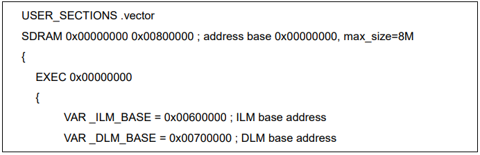
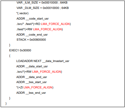 Figure 9. “LMA_FORCE_ALIGN” example
Figure 10 is the ELF header generated after project compilation with the SaG file in Figure 9. In this figure, we can see that the LMA of the .sbss_b section is changed from 0x1d42 to 0x1d44.
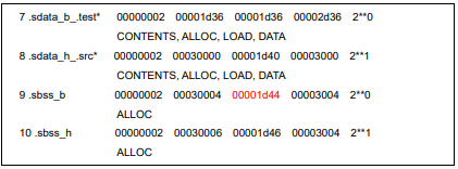 Figure 10. Result of using “LMA_FORCE_ALIGN”
5. Conclusion
Andes provides programmers with the easy-to-use SaG tool to replace the complex linker scripts, thereby significantly improving their software development efficiency on AndesCore platform. This paper demonstrates the competent and friendly Andes SaG tool by real examples that solve engineering problems efficiently. As the SaG tool gets more and more powerful, we would like developers to get deeper understanding of its functional design – this is actually what the last example aims for. We look forward to seeing more developers mastering Andes SaG tool and hearing more about how this tool helps to tackle software development problems agilely.
Reference document:
1: Andes Programming Guide for BSP v3.2.1 (Linker Script Generator chapter)
2: The GNU Linker Manual
Put on the Future: Wearable Technology
1. Introduction
While jogging, your shoes can record your running speed, acceleration, path and distance. While taking a subway, the ring you wear can display how far your train is and how soon it will come; it also shows you at which stop you should take a transfer and when the next train will arrive. While putting on your mask in a city with poor air quality, your mask not only protects you, but it also detects and shares the air quality data to the cloud so that everybody can see air quality anywhere in the city on the display of his/her mobile phone. All of these are not just scenarios, but they have become real. Wearable technology has been widely adopted in various end-use segments and become a part of our daily life.
2. Market TAM, forecast, and trend
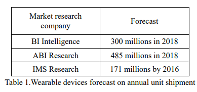
Even though wearable technology is in its early stage, it has reached 14 millions pieces of annual device shipment in 2011 according to IMS Research, and is forecasted to have a rapid growth to 171 millions by 2016. Other researches confirmed the same direction with even more optimistic forecast (Table 1). The market size will reach USD 5.8 billion in 2018 at CAGR of 40.8% from 2012 to 2018 predicted by Transparency Market Research. A large portion of shipment will be in the categories of healthcare, medical, wellness, and sport/fitness; the industrial and military usage will also occupy a certain portion. However, the emerging Infotainment products such as Smart Glasses and Smart Watches are projected to have a higher growth rate and will surpass the other products to become the major revenue contributor to the entire wearable industry in the future. Though some other subsidiary segments such as fashion, gaming, etc. are relatively smaller now, with more and more innovative products coming out they also have good potential to become big and deserve continuous attention.
Some key players in their respective segments have adopted wearable technology into their product lines to help growing the market. For example, the leading companies in sports goods such as Adidas and Nike have wearable products ready in the fields of health and wellness. The wearable market growth is also driven by some other factors. First, mobile phones play the role of personal hubs to connect wearable devices through wireless technology like Bluetooth and provide the capability of online data access. This makes many products and applications in the field of mobile monitors/trackers feasible and successful. As a result, the demand is not only on devices but also on aggregators, cloud service, operators and the whole ecosystem gets major boost. Furthermore, the participation of big software companies such as Google, Apple, Microsoft, and Facebook provides platforms to integrate various services. It is definitely a driving engine to accelerate the entire industry toward maturity. Nevertheless, the advances in material science, power-efficient components, battery life, sensor technology, and SoC evolution can not be overlooked. They will make wearable devices thinner, lighter, more durable, portable and less power hungry, and these features are the keys to make them easily embedded into our daily life and accepted by the market. All these together drive the market growth in a tremendously rapid way.
3. Requirements
To ensure the success of a new wearable device, it has to meet at least two basic requirements from technology viewpoint: compactness and portability. In order to achieve compactness, each component of the device should be selected as small as possible, including the battery. Regarding to portability, power efficiency should be the most important consideration because it eliminates the need of frequent battery re-charging.
Therefore, choosing small size and power efficient components will be the fundamental challenge for engineering.
4. AndesCore™ embedded body sensor network
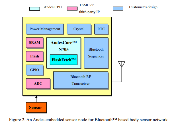
Body sensor network plays very important role in wearable products, especially in medical and healthcare applications. Bluetooth is one of the best candidates for wireless body sensor network of wearable products because it has become a standard feature in mobile phones for short range communication. The Bluetooth protocol provides point to point and point to multi-point mechanisms that can be used for the mobile phone to efficiently communicate with individual sensor nodes worn on the human body. Sensor devices can gather the desired information and perform basic processing; then the results are sent to a mobile phone to undertake further calculation and statistics gathering (Figure 1). Users can install APPs to their mobile phones to display medical data in an easy-to-digest format.
Furthermore, users can use the APPs to transmit the data to the server of remote medical care systems or cloud computing environments to have more accurate diagnosis.

Figure 1. Body sensor network connecting to mobile phone device
Andes Technology Corporation, a dedicated vendor of 32-bit CPU IP and associated SoC platforms, provides the innovated performance-efficient processor solution for SoC. To serve the requirements of Bluetooth based sensor nodes with competitive low power and small size, Andes architects a solution implementing the AndesCore™ configurable 32-bit CPU IP N705 with TSMC 90nm Low Power process and its related IP.
The AndesCore™ N705 is an ultra power-efficient compact synthesizable softcore of a general-purpose 32-bit embedded processor. For ease of integration in SoC design, the N705 is delivered with a complete softcore development package as well as reference design flow to fit customer’s requirements in all aspects of performance, power consumption, and die area. In addition, it supports All-C Embedded Programming, C libraries optimized for MCUs and low-cost ICE debugger through Serial Debug Port (SDP). With TSMC’s world-class technology in processes and supporting infrastructure, the N705 demonstrates the industry-leading power efficiency at 90LP for a 32-bit CPU core using TSMC standard library. It achieves over 100 DMIPS/mWatt, or 115 to be exact. The N705 uses as little as 12K gates logic and can deliver up to 1.51 DMIPS/MHz and 2.62 CoreMark/MHz. Both are the industry leading scores for CPUs at this level.
N705 can be connected to the slow and power-hungry embedded flash memory directly. Thanks to the FlashFetch™ technology, the N705 can not only run in its full speed, but also help reduce flash power consumption significantly by avoiding over 50% flash instruction memory accesses in EEMBC’s CoreMark® benchmark. Both together ensure ultra power efficiency in the real world environment. Under 2:1 CPU vs Flash speed ratio, the N705 demonstrates 37% higher power efficiency (DMIPS/mWatt) and still maintains 11% better area efficiency (DMIPS/mm2) over the leading supplier’s smallest and lowest power CPU core. The N705 supports flexible power management mechanism through software, but it can also relinquish the control to the SoC through a standby request input signal. This allows SoCs to fulfill the requirements of versatile power management modes. The following block diagram (Figure 2) shows an example of an AndesCore™ N705 based Bluetooth SoC supporting sensor network. This SoC combines Andes CPU IP, TSMC standard cell and libraries, TSMC or the third party IP including embedded flash, SRAM macro and ADC. The sensor would get the analog signals from the human body and ADC would convert the analog signals to their digital counterparts that can be handled by the CPU for basic analysis. The analysis results will be transmitted through the Bluetooth protocol logic and transceiver to the mobile phone, where the application program would present the data in an easy-to-understand format.
5. Conclusion
Wearable technology and products intimately bind our lives to healthcare, medical, wellness, sports and fitness, and lead us to better, healthier and more convenient life. It forms an industry with a high growth potential. The wearable products will have an annual growth of over 40% for the next 6 years to reach the total revenue of over USD 5 billion in 2018. Part of their success depends on its mean time between battery charges. Andes Technology would like to contribute to the industry by offering AndesCore™ N705 together with TSMC’s advanced processes and libraries to serve the demanding SoCs with the best power consumption, efficiency and small die size.
Note: FlashFetch™, AndeStar™, and AndesCore™ are trademarks of Andes Technology Corporation. CoreMark® is the CPU core benchmark developed by EEMBC organization.
An Introduction to the AndesCore™ N705 processor
1. Introduction
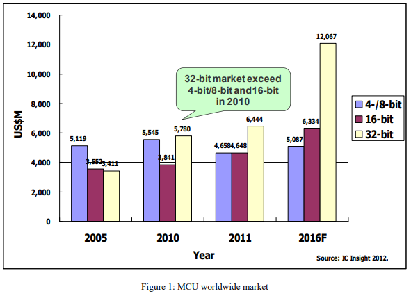
The 32-bit MCU is in a fast growing market. Its 13% compound annual growth rate (CAGR) from 2010 to 2016 is higher than the 8% CAGR of the total MCU market. The revenue of 32-bit MCU exceeded that of 4-bit/8-bit/16-bit MCU’s in 2010, and will be more than 50% of the total MCU market share in 2016 (Figure 1).
The AndesCore™ N705 is an ultra power-efficient compact synthesizable softcore of a general-purpose 32-bit embedded processor. With low gate count, high power-efficiency, high configurability and AndeStar™ V3m ISA’s small code size, it is the best candidate to replace 8051 and other 8-bit MCU’s for small-footprint, cost and power and energy sensitive applications.
For ease of integration in SoC design, the N705 is delivered with a complete softcore development package as well as reference design flow to fit customer’s requirements in all aspects of performance, power consumption, and die cost. In addition, since the N705 is binary-compatible with the existing popular N801, it is immediately supported by user-friendly development tools, All-C Embedded Programming, size-optimized MCU libraries and Serial Debug Port (SDP)-based low-cost ICE debugger, already there for N801.
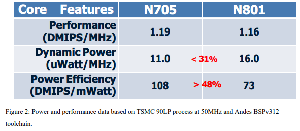
2. Power, performance and area
The creation of the N705 was inspired by the feedbacks from some customers of N801, the previous most power-efficient AndesCore™. Their applications have more than enough total performance, but they looked to cut power and energy consumption further. The results are shown in Figure 2. Compared to N801, the N705 has a 31% lower dynamic power, slightly improved per-MHz performance, and the resulting almost 50% higher power efficiency. That leads to the industry-leading power efficiency at 90nm of over 100 DMIPS/mWatt, or 108 to be exact. This is impressive especially when the N705 delivers this with foundry’s standard library. The N705 at its minimum configuration uses as little as 12K gates while a full-configured N705 can reach 1.45 DMIPS/MHz and 2.28 CoreMark/MHz.
3. Architecture and features
The N705 has a 2-stage streamlined pipeline based on 16-bit/32-bit mixable AndeStar™ V3m architecture. Its basic features include 16 general-purpose registers, 16MB address space, multiplier with small area, hardware divider, AHB-lite bus and two-wire debug interface. It also supports AndeStar’s standard power management flow.
It also provides the alternative 1-cycle multiplier and 1-cycle Instruction/Data Local Memory (ILM/DLM) interface options. The increased parallelism through ILM or DLM allows simultaneous instruction fetches and data accesses, resulting in higher performance. For 8-bit MCU users who like to stick to SRAM-based peripheral interfaces, either ILM or DLM can be used because all their accesses are non-speculative. The N705 also offers Serial Debug Port (SDP), Andes’ 2-wire debug interface. SDP allows an N705-embedded SoC to use Andes’ low-cost ICE, AICE-mcu.
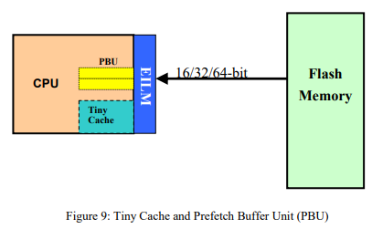
With built-in vector interrupt controller, it supports nested interrupts with 4 programmable priorities and up to 32 direct interrupt sources. For SoC design’s consideration, it provides N:1 CPU-to-bus clock ratio option and thus additional means for power saving. It also offers optional Tiny Cache and Prefetch Buffer Unit to connect to the lower-speed and power-hungrier flash memory to allow the N705 to run in its full speed and reduce flash power on repeated code, (Figure 3).

3.1 V3m architecture
AndeStar™ V3 ISA is based on V2 ISA, plus 38 new instructions, therefore V3 is backward compatible to V2 ISA. V3m is the subset of V3 and its instructions are selected from the most commonly used ones for MCU applications. In addition to vector interrupt architecture, it supports priority-based preemption, including 4 priorities and built-in interrupt controller for up to 32 interrupt sources. The operation is
if (Global Interrupt Enable is turned on)
if (current priority < incoming priority)
allow execution to switch to the handler for the incoming interrupt;
else
let incoming wait;
All-C Embedded Programming is another major benefit for V3 and V3m architecture. Software engineers can program startup function and ISR (Interrupt Service Routine) in pure C language and gain higher productivity and lower maintenance. It is done with attributes attached to the function definitions or declarations as follows:
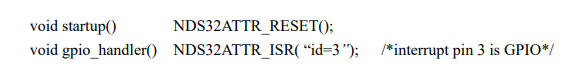
Compiler will automatically generate required code sequence based on the attributes.
3.2. Smaller code size
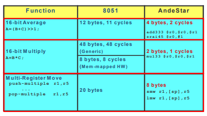
More and more MCU applications require the precision of 16-bit ADC. As a result, computations involved also need to handle the 16-bit data, and the temporary data may need to go up to 32 bits. The trend in moving to 16-bit and 32-bit computations and data exposes the performance deficiency of 8-bit MCU’s and wipe out their past code size advantages. The following table highlights some typical examples between AndeStar and 8051. The first two examples show the advantage of AndeStar’s 32-bit registers and computations over 8051’s 8-bit ones. Besides, AndeStar’s patented instructions for multiple register pushes to memory and pops from memory support frequently-used functions for stack push/pop and memory copies. The rich semantics is difficult, if not impossible, to encode into the limited encoding space of 8-bit CPU’s.
3.3. Power management flow
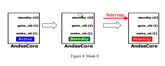
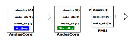
The N705 supports power management mechanism through either software or standby request input pin. “STANDBY” instruction can be used to initiate a power management control sequence for three different modes. It uses two associated IO signals: standby and wakeup_ok. The three standby modes and their associated usage scenarios are as follows:
Standby mode0
When the SW is idling, the standby instruction with mode 0 can be executed. After all CPU’s outstanding requests are finished, the CPU core will clock-gate all except a very small portion of its logic. When an interrupt arrives, the CPU resumes its execution.
Mode 1: When the SW decides to change its operating condition (e.g. frequency and voltage) and continues execution, the standby instruction with mode 1 can be used. The CPU core will assert signal standby and clock-gate itself. An external PMU can start adjusting the operating condition, and when it is done, the PMU will send a signal to wake up the CPU.

Mode2: When the SW wants to change its operating condition and waits for interrupt to resume its execution, it can execute the standby instruction with mode 2. It proceeds similarly to mode 1. Except when receiving PMU’s wakeup signal, the small portion logic in the CPU starts monitoring interrupt requests. Any interrupt will take the CPU core out of the standby mode to resume execution.
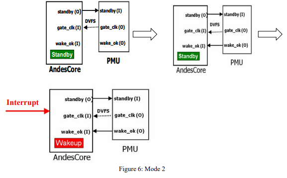
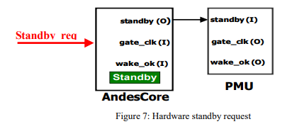
Another way for an AndesCore to enter standby mode is to use the standby_req input signal. After standby_req signal is asserted, AndesCore behaves similarly to the execution of a STANDBY instruction in Mode 1. (Figure 7)
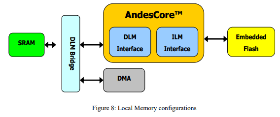
3.4. Local Memory interface
The N705 provides SRAM-like Instruction and Data Local Memory interface up to 1MB. It also provides mechanism with related signals to support wait cycle for lower speed Local Memory. Those two major signals are ExLM_wait_cnt signal and ExLM_wait signal and work together to stall CPU internal pipeline. Signal ExLM_wait_cnt is used when the wait cycles are fixed. For example, when the Local Memory is only connected to the CPU, the internal pipeline will be stalled based on ExLM_wait_cnt information (0=no stall, 1=stall one clock, 2=stall 2 clocks, 3=stall 3 clocks). It reduces SoC’s burden of housekeeping the fixed latency of the Local Memory.
On the other hand, if the Local Memory is shared between the CPU and other SoC logic such as DMA devices, signal ExLM_wait could be used. It is serves as a wait state indication from the Local Memory if it can not accept the CPU’s read/write request in the next cycle. Once the ExLM_wait signal is de-asserted, the CPU is allowed to send out the next request in the next cycle.
Without PBU (covered later), ILM supports 32-bit width as well as 16-bit width to allow flexible tradeoff on cost, performance and power for SoC’s.
3.5. Prefetch Buffer (PBU) and Tiny Cache
Flash memory is a very commonly-used embedded memory for program code in MCU’s, due to its ability to keep the contents even when the power goes off. But, it usually has lower speed and higher power consumption comparing with CPU core. In order to fully utilize the CPU performance and reduce the power to access flash memory, the N705 provides optional Prefetch Buffer Unit (PBU) and Tiny Cache to address this. PBU brings the subsequent instructions into a small buffer before the CPU makes the request. It hides the latency of flash memory while CPU is reading the current instruction (Figure 9). The prefetch width of PBU can be configured to 32 bits and 64 bits depending on applications. Tiny Cache uses a buffer larger than PBU, but much smaller than the traditional caches to exploit program’s locality on repeated code. It can reduce accesses to the instruction memory by over 50% and thus cut energy consumption for instruction memory accesses by half. Performance is also improved as a result.
3.6. Secured debugging
Program code and data protection becomes very important in the current SoC design. The N705 provides secured debugging mechanism to prevent the unauthorized persons to access the contents. In the debug mode, an output signal debug_access from the CPU core is asserted. It can be used to restrict CPU’s accesses to the SoC address space and full accesses can be enabled after a certain sequence is exercised.
4. Development tools and debugging
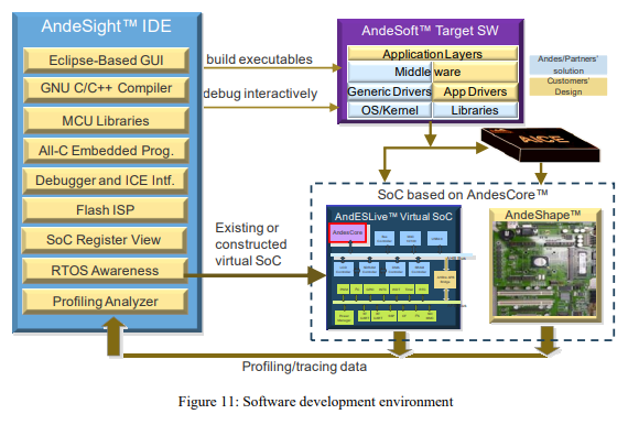
Andes’ software development environment AndeSight™ is an Eclipse based integrated graphical user interface development environment (Figure 10). For program development, it provides the highly-optimized compiler, the All-C Embedded Programming environment, and optimized C libraries for MCU applications. For debugging and performance tuning, it offers Memory view and SoC Register view, RTOS task/resource view, function-level profiling, and ICE connection. It allows stopping and single stepping through an interrupt routine. It also supports customizable flash ISP (In System Programming).
Software engineers can develop application programs with RTOSes and middlewares ported to AndeStar architecture, which include open-sourced FreeRTOS, eCos and Contiki, and commercial uC/OS (II and III), Thread-X, uITRON, and Nucleus. In addition, they can use FPGA development board or simulator for program development and verification, (Figure 11).

5. Summary
The 2-stage pipeline AndesCore N705 provides not only the ultra power efficiency but also a complete MCU solution. It is designed for cost and power sensitive applications like smart meters, Internet of Things, medical devices, sensor applications, wearable devices, etc. and is the best candidate to replace 8-bit/16-bit MCU’s.
