The Defense Advanced Research Projects Agency (DARPA) recently set a goal to design a 200-million transistor chip in 30 weeks with a 10-person team. DARPA expects to achieve this result through “increased reuse and lowered level of manpower and design expertise required to design and verify integrated circuits in leading-edge CMOS technology…“ according to the PDF at DARPA site*, Design reuse is the mainstay of SoCs going into consumer devices, automotive electronics, communications, and data center applications. It involves large collections of third party IP, applications processors, GPUs, DSPs, and more tied together by a high-speed on-chip bus fabric.
In addition to the computing resources, these SoCs also require memory controllers and any number of peripherals—PCI Express, NVM Express, MIPI, HDMI, SPI, PVT (process, voltage, temperature sensors), among others. Each of these elements comes with control signals such as error messages, status updates, etc. that need to be connected to logic or a stage machine to perform some function. In SoCs with multiple special processors all running independently and communicating with one another, monitoring their operation is even more difficult. Significant glue logic and state machines stitch together these many third party blocks into the larger design, creating significant design and verification overhead.
This glue logic and state machines have significant drawbacks. Foremost is the time and effort expended developing something that is not an integral part of the value-add of the final chip.
Next, any error or oversight in these circuits could cause a costly design spin and deployment risk. Finally, designing all of this in hardware significantly restricts the ability to make changes post-silicon. For example, something as simple as the boot sequence of when to power-up the various processors in the design is permanently fixed in a state machine. Any change in this sequence post silicon requires a design spin. These problems can be resolved if instead of glue logic and state machines, a system control processor is designed into the SoC to provide a form of SoC control intelligence—a personal assistant for all the elements on the SoC.
Value of a System Control Processor
The system control processor can execute functions in software that would otherwise be done by hardware logic. This is accomplished by connecting all the signals from third party IP blocks that are not directing the flow of data to and from the main applications processor to an on-chip microcontroller and writing software to manage these signals—buffer overflow, crc error, etc.
Having a system control processor to handle the status and control signals that are not required for the flow of data through peripherals and interfaces of the SoC design, total performance of the application process can be improved.
What are the benefits of this solution? The most compelling benefit is that software provides the design team the “do over” benefit, without requiring a hardware spin. Another benefit comes from adding intelligence to the operating control of the chip. Transferring all the status and control functions not essential to the main mission of the applications processor to a system control processor can help save power while improving the performance of the system. Another example is the boot sequence. If after the chip is fabricated the sequence needs to be altered it can be done with a simple software change. Managing power is another real benefit. PC vendors often update their BIOS to improve power management. A system control processor can offer the same flexibility at the SOC level. Rules for powering down or shutting off elements can be changed to improve system performance post silicon.
A Complete Platform for System Control
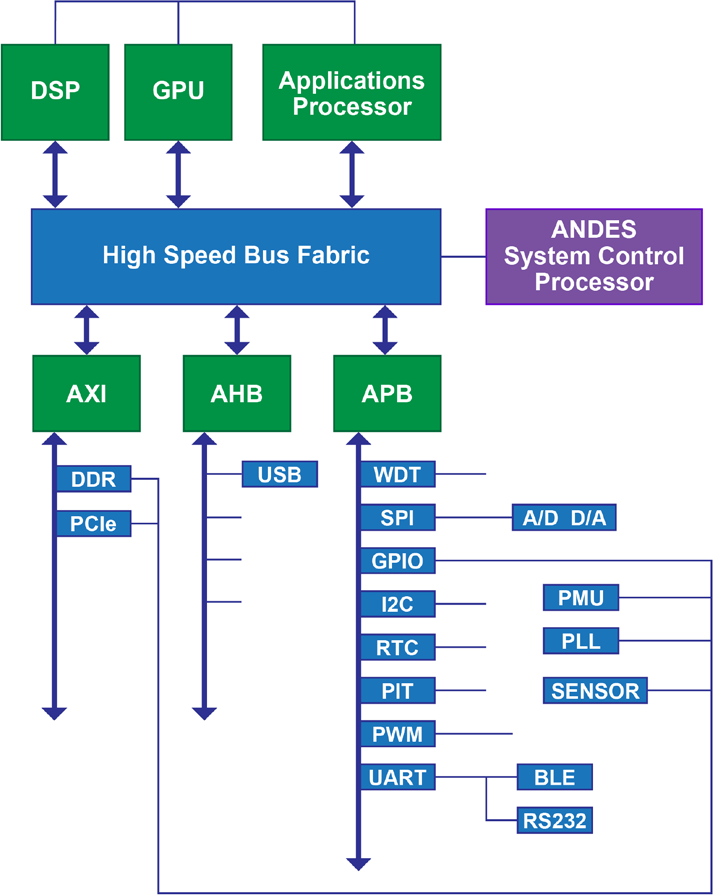
Incorporating a system control processor into a larger SoC design still requires integrating the memory and peripherals commonly found on all processors. Andes Technology Corporation has developed a platform for system control to reduce the effort of assembling these elements and the platform provides a more complete solution for SoC designers wanting to adopt the system control processor solution. The platform includes a system control processor core to monitor and control the operation of the SoC (see Figure) and the peripherals and bus fabric required by a typical SoC design. A complete software development package with demo examples is included to jump-start the programming of the embedded processor.
The bus fabric is an important part of platform, since it provides the ready-made communication link between the major compute engines of the SoC and its memory and peripherals elements. The bus fabric supplied in the platform is optimized for ease of use while being cost competitive.
It has an AXI, AHB, and APB fabric with configurable numbers of masters and slaves. In addition to the bus fabric and the Andes system control processor, the platform comes with a set of peripherals to provide the most common functions in a typical SoC design: SRAM bridge, GPIO, SPI, watchdog timer, programmable interval timer, and UART. Designers are freed from integrating these essential functions so they can concentrate on their value added design.
For designers wanting to reduce their design and silicon re-spin risk while enabling greater design flexibility once a design is in silicon, the Andes platform for system control provides a cost-effective solution. The platform comes fully assembled with software modules pre-packaged. Incorporating additional elements is a straightforward addition to the design and the creation of software code to interpret the sensor reading and act on the findings. And software development can be done in C code, making changes before and after silicon a simple program change, thus reducing risk and enhancing design flexibility.