1. Introduction
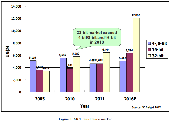
The 32-bit MCU is in a fast growing market. Its 13% compound annual growth rate (CAGR) from 2010 to 2016 is higher than the 8% CAGR of the total MCU market. The revenue of 32-bit MCU exceeded that of 4-bit/8-bit/16-bit MCU’s in 2010, and will be more than 50% of the total MCU market share in 2016 (Figure 1).
The AndesCore™ N705 is an ultra power-efficient compact synthesizable softcore of a general-purpose 32-bit embedded processor. With low gate count, high power-efficiency, high configurability and AndeStar™ V3m ISA’s small code size, it is the best candidate to replace 8051 and other 8-bit MCU’s for small-footprint, cost and power and energy sensitive applications.
For ease of integration in SoC design, the N705 is delivered with a complete softcore development package as well as reference design flow to fit customer’s requirements in all aspects of performance, power consumption, and die cost. In addition, since the N705 is binary-compatible with the existing popular N801, it is immediately supported by user-friendly development tools, All-C Embedded Programming, size-optimized MCU libraries and Serial Debug Port (SDP)-based low-cost ICE debugger, already there for N801.
2. Power, performance and area
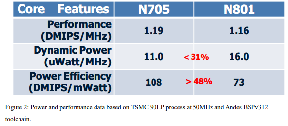
The creation of the N705 was inspired by the feedbacks from some customers of N801, the previous most power-efficient AndesCore™. Their applications have more than enough total performance, but they looked to cut power and energy consumption further. The results are shown in Figure 2. Compared to N801, the N705 has a 31% lower dynamic power, slightly improved per-MHz performance, and the resulting almost 50% higher power efficiency. That leads to the industry-leading power efficiency at 90nm of over 100 DMIPS/mWatt, or 108 to be exact. This is impressive especially when the N705 delivers this with foundry’s standard library. The N705 at its minimum configuration uses as little as 12K gates while a full-configured N705 can reach 1.45 DMIPS/MHz and 2.28 CoreMark/MHz.
3. Architecture and features
The N705 has a 2-stage streamlined pipeline based on 16-bit/32-bit mixable AndeStar™ V3m architecture. Its basic features include 16 general-purpose registers, 16MB address space, multiplier with small area, hardware divider, AHB-lite bus and two-wire debug interface. It also supports AndeStar’s standard power management flow.
It also provides the alternative 1-cycle multiplier and 1-cycle Instruction/Data Local Memory (ILM/DLM) interface options. The increased parallelism through ILM or DLM allows simultaneous instruction fetches and data accesses, resulting in higher performance. For 8-bit MCU users who like to stick to SRAM-based peripheral interfaces, either ILM or DLM can be used because all their accesses are non-speculative. The N705 also offers Serial Debug Port (SDP), Andes’ 2-wire debug interface. SDP allows an N705-embedded SoC to use Andes’ low-cost ICE, AICE-mcu.
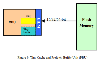
With built-in vector interrupt controller, it supports nested interrupts with 4 programmable priorities and up to 32 direct interrupt sources. For SoC design’s consideration, it provides N:1 CPU-to-bus clock ratio option and thus additional means for power saving. It also offers optional Tiny Cache and Prefetch Buffer Unit to connect to the lower-speed and power-hungrier flash memory to allow the N705 to run in its full speed and reduce flash power on repeated code, (Figure 3).

3.1 V3m architecture
AndeStar™ V3 ISA is based on V2 ISA, plus 38 new instructions, therefore V3 is backward compatible to V2 ISA. V3m is the subset of V3 and its instructions are selected from the most commonly used ones for MCU applications. In addition to vector interrupt architecture, it supports priority-based preemption, including 4 priorities and built-in interrupt controller for up to 32 interrupt sources. The operation is
if (Global Interrupt Enable is turned on)
if (current priority < incoming priority)
allow execution to switch to the handler for the incoming interrupt;
else
let incoming wait;
All-C Embedded Programming is another major benefit for V3 and V3m architecture. Software engineers can program startup function and ISR (Interrupt Service Routine) in pure C language and gain higher productivity and lower maintenance. It is done with attributes attached to the function definitions or declarations as follows:
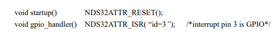
Compiler will automatically generate required code sequence based on the attributes.
3.2. Smaller code size
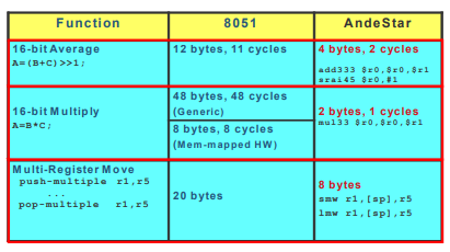
More and more MCU applications require the precision of 16-bit ADC. As a result, computations involved also need to handle the 16-bit data, and the temporary data may need to go up to 32 bits. The trend in moving to 16-bit and 32-bit computations and data exposes the performance deficiency of 8-bit MCU’s and wipe out their past code size advantages. The following table highlights some typical examples between AndeStar and 8051. The first two examples show the advantage of AndeStar’s 32-bit registers and computations over 8051’s 8-bit ones. Besides, AndeStar’s patented instructions for multiple register pushes to memory and pops from memory support frequently-used functions for stack push/pop and memory copies. The rich semantics is difficult, if not impossible, to encode into the limited encoding space of 8-bit CPU’s.
3.3. Power management flow
The N705 supports power management mechanism through either software or standby request input pin. “STANDBY” instruction can be used to initiate a power management control sequence for three different modes. It uses two associated IO signals: standby and wakeup_ok. The three standby modes and their associated usage scenarios are as follows:
Standby mode0
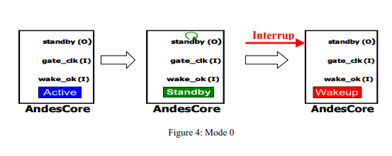
When the SW is idling, the standby instruction with mode 0 can be executed. After all CPU’s outstanding requests are finished, the CPU core will clock-gate all except a very small portion of its logic. When an interrupt arrives, the CPU resumes its execution.
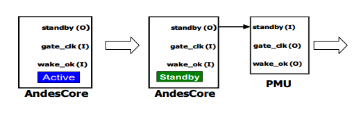
Mode 1: When the SW decides to change its operating condition (e.g. frequency and voltage) and continues execution, the standby instruction with mode 1 can be used. The CPU core will assert signal standby and clock-gate itself. An external PMU can start adjusting the operating condition, and when it is done, the PMU will send a signal to wake up the CPU.

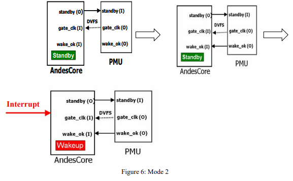
Mode2: When the SW wants to change its operating condition and waits for interrupt to resume its execution, it can execute the standby instruction with mode 2. It proceeds similarly to mode 1. Except when receiving PMU’s wakeup signal, the small portion logic in the CPU starts monitoring interrupt requests. Any interrupt will take the CPU core out of the standby mode to resume execution.
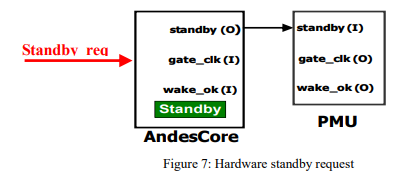
Another way for an AndesCore to enter standby mode is to use the standby_req input signal. After standby_req signal is asserted, AndesCore behaves similarly to the execution of a STANDBY instruction in Mode 1. (Figure 7)
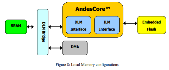
3.4. Local Memory interface
The N705 provides SRAM-like Instruction and Data Local Memory interface up to 1MB. It also provides mechanism with related signals to support wait cycle for lower speed Local Memory. Those two major signals are ExLM_wait_cnt signal and ExLM_wait signal and work together to stall CPU internal pipeline. Signal ExLM_wait_cnt is used when the wait cycles are fixed. For example, when the Local Memory is only connected to the CPU, the internal pipeline will be stalled based on ExLM_wait_cnt information (0=no stall, 1=stall one clock, 2=stall 2 clocks, 3=stall 3 clocks). It reduces SoC’s burden of housekeeping the fixed latency of the Local Memory.
On the other hand, if the Local Memory is shared between the CPU and other SoC logic such as DMA devices, signal ExLM_wait could be used. It is serves as a wait state indication from the Local Memory if it can not accept the CPU’s read/write request in the next cycle. Once the ExLM_wait signal is de-asserted, the CPU is allowed to send out the next request in the next cycle.
Without PBU (covered later), ILM supports 32-bit width as well as 16-bit width to allow flexible tradeoff on cost, performance and power for SoC’s.
3.5. Prefetch Buffer (PBU) and Tiny Cache
Flash memory is a very commonly-used embedded memory for program code in MCU’s, due to its ability to keep the contents even when the power goes off. But, it usually has lower speed and higher power consumption comparing with CPU core. In order to fully utilize the CPU performance and reduce the power to access flash memory, the N705 provides optional Prefetch Buffer Unit (PBU) and Tiny Cache to address this. PBU brings the subsequent instructions into a small buffer before the CPU makes the request. It hides the latency of flash memory while CPU is reading the current instruction (Figure 9). The prefetch width of PBU can be configured to 32 bits and 64 bits depending on applications. Tiny Cache uses a buffer larger than PBU, but much smaller than the traditional caches to exploit program’s locality on repeated code. It can reduce accesses to the instruction memory by over 50% and thus cut energy consumption for instruction memory accesses by half. Performance is also improved as a result.
3.6. Secured debugging
Program code and data protection becomes very important in the current SoC design. The N705 provides secured debugging mechanism to prevent the unauthorized persons to access the contents. In the debug mode, an output signal debug_access from the CPU core is asserted. It can be used to restrict CPU’s accesses to the SoC address space and full accesses can be enabled after a certain sequence is exercised.
4. Development tools and debugging
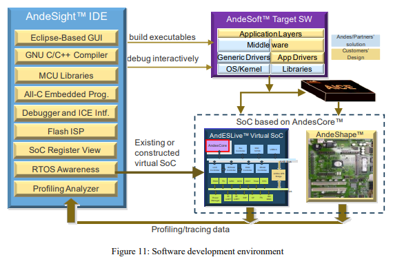
Andes’ software development environment AndeSight™ is an Eclipse based integrated graphical user interface development environment (Figure 10). For program development, it provides the highly-optimized compiler, the All-C Embedded Programming environment, and optimized C libraries for MCU applications. For debugging and performance tuning, it offers Memory view and SoC Register view, RTOS task/resource view, function-level profiling, and ICE connection. It allows stopping and single stepping through an interrupt routine. It also supports customizable flash ISP (In System Programming).
Software engineers can develop application programs with RTOSes and middlewares ported to AndeStar architecture, which include open-sourced FreeRTOS, eCos and Contiki, and commercial uC/OS (II and III), Thread-X, uITRON, and Nucleus. In addition, they can use FPGA development board or simulator for program development and verification, (Figure 11).

5. Summary
The 2-stage pipeline AndesCore N705 provides not only the ultra power efficiency but also a complete MCU solution. It is designed for cost and power sensitive applications like smart meters, Internet of Things, medical devices, sensor applications, wearable devices, etc. and is the best candidate to replace 8-bit/16-bit MCU’s.
