Andes Technology Showcases Leadership in AI and Automotive Applications at RISC-V Summit Europe 2024
- Post author:Peng Murphy
- Post published:2024-06-21
- Post category:Press Release
Industry-leading RISC-V solutions and live demonstrations of CPU IP are all on display at Booth #8. Discover the latest advancements from Andes’ presentations and posters!
Munich, Germany – June 21, 2024 – Andes Technology Corporation, a leading provider of high efficiency, low-power 32/64-bit RISC-V processor cores and a Founding Premier member of RISC-V International, is pleased to announce its participation in RISC-V Summit Europe 2024, the prestigious annual event held from June 24 to 28, 2024, in Munich. As a significant contributor, Andes will have presentations to highlight its comprehensive lineup of RISC-V IP and also feature its cutting-edge RISC-V development in the poster session. Andes will demonstrate its leadership in AI and automotive technology as well as showcase the latest QiLai SoC and its development board for RISC-V SW development at booth #8.
Frankwell Lin, Andes Chairman and CEO, will spotlight Andes RISC-V IP portfolio, robust partner ecosystem and latest processors, including an automotive-grade ISO26262 certified core and an out-of-order CPU in the demo theatre speech “Andes High Value RISC-V Processors and Their Applications” on June 25 at 1:10 PM. Chun-Nan Ke, Andes Senior Technical Manager, will delve into how matrix extension and customized quantization instructions for RISC-V can improve general convolutional neural network (CNN) applications in his presentation “Enhancing Convolutional Neural Network Computation with Integrated Matrix Extension” on June 25 at 12:15 PM. Lastly, Vince Wu, Andes Sales Manager, will share compelling customer success stories in the demo talk “Andes RISC-V, Everywhere in Our Life!” on June 25 at 4:20 PM.
Andes, playing a crucial role in the RISC-V community, will exhibit four posters at the poster session. The topics covered include Andes’ ecosystem approach to drive RISC-V adoption in automotive, insights into IOPMP, MobileBERT on RISC-V, and integrated matrix extension. Visit and engage with Andes speakers to gain deeper insights into how these technologies are shaping and revolutionizing RISC-V computing.
The display of QiLai SoC and the Voyager development board will be one of the highlights of the event. The QiLai SoC includes high performance quad-core RISC-V AX45MP cluster and one NX27V vector processor. The Voyager is a 9.6” x 9.6” Micro ATX form factor development board including a QiLai SoC and a multitude of peripherals. The AndesCore™ AX45MP superscalar multicore contains a 2MB Level-2 cache and a MMU (Memory Management Unit) for Linux based applications. The AndesCore™ NX27V vector processor supports a full range of RISC-V standard data types and Andes-enhanced data types optimized for AI workloads. Manufactured at TSMC advanced 7nm process technology, the QiLai SoC and its Voyager development board demonstrate live Andes’ commitment to enable RISC-V software development. The QiLai SoC and the Voyager development board will be exhibited at both Andes booth and the Developer Zone. Take this opportunity to witness the premiere of Andes cutting-edge RISC-V technology.
In addition, Andes will proudly showcase development boards with AndesCore-based SoC from customers at booth #8. These boards include the Tinker V, the first RISC-V Single-Board Computer (SBC) from ASUS IoT; an MPU development board from Renesas; an AI development kit with a camera module from Canaan. Visit booth #8 to engage in one-on-one discussion with Andes experts and experience live demonstrations of advanced CPU IP technology.
Details of Andes’ sessions during the RISC-V Summit Europe are as follows:
June 25, Tuesday
- 12:15-12:30 PM: Presentation “Enhancing Convolutional Neural Network Computation with Integrated Matrix Extension” by Chun-Nan Ke, Senior Technical Manager
- 1:10-1:20 PM: Demo Theatre Talk “Andes High Value RISC-V Processors and Their Applications” by Frankwell Lin, Chairman and CEO
- 4:20 PM: 2′ Lightning Talk “Andes RISC-V, Everywhere in Our Life!” by Vince Wu, Sales Manager
- All day: Poster “Andes’ Ecosystem Approach to Drive RISC-V Adoption in Automotive Designs” by Samuel Chiang, Deputy Marketing Director
- All day: Poster “Deep Insight into IOPMP: Priority and Non-Priority Rules” by Paul Ku, Deputy Director
June 27, Thursday
- All day: Poster “MobileBERT on RISC-V: Leveraging IREE Compiler and ACE-RVV Extension for Softmax Acceleration” by Yueh-Feng Lee, Manager of Compute Acceleration Division
- All day: Poster “Enhancing Convolutional Neural Network Computation with Integrated Matrix Extension” by Chun-Nan Ke, Senior Technical Manager
For more information, please visit the RISC-V Summit Europe website.
About Andes Technology
Nineteen years in business and a Founding Premier member of RISC-V International, Andes is a publicly-listed company (TWSE: 6533; SIN: US03420C2089; ISIN: US03420C1099) and a leading supplier of high-performance/low-power 32/64-bit embedded processor IP solutions, and the driving force in taking RISC-V mainstream. Its V5 RISC-V CPU families range from tiny 32-bit cores to advanced 64-bit Out-of-Order processors with DSP, FPU, Vector, Linux, superscalar, functional safety and/or multi/many-core capabilities. By the end of 2023, the cumulative volume of Andes-Embedded™ SoCs has surpassed 14 billion. For more information, please visit https://www.andestech.com. Follow Andes on LinkedIn, Twitter, Bilibili, and YouTube! !


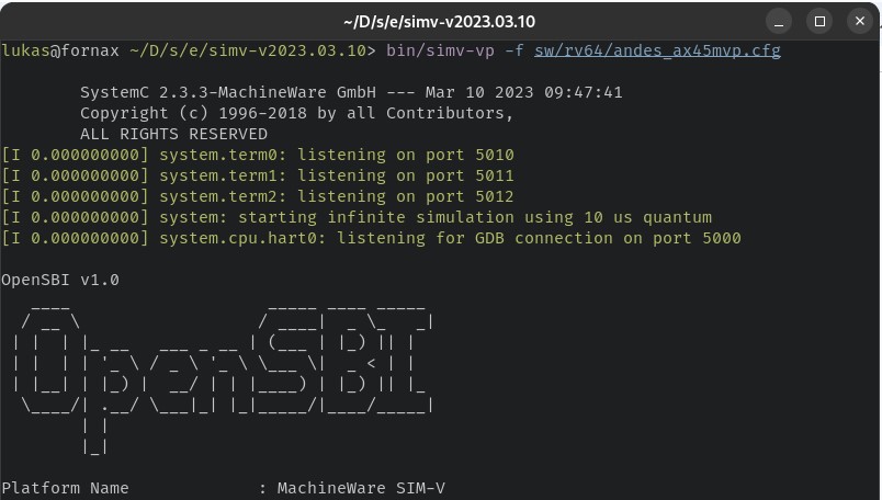
 Figure 1: Invoking SIM-V with the AX45MPV configuration.