General Description
ADP-XC7K160/410 is a multi-purpose development and prototyping board that provides rich capacity for evaluation of variety of AndesCore™ processors and AndeShape™ SoC platform IPs. It works with AndeSight™ software development suites and AICE in-circuit debugging tools. It also utilizes Xilinx Kintex 7 FPGA built-in hi-speed I/Os to support DDR3* and PCI-E interface for better system performance.
ADP-XC7K160/410 supports numerous peripheral interfaces and allows developers to add expansion cards for custom peripherals and devices. Developers can test and optimize the hardware and software components with a fast turnaround time between system designs, hence reducing development time, cost, and risk. Please note that Figure 1 shows the green PCB is ADP-XC7K160 and Figure 2 shows the red PCB is ADP-XC7K410.
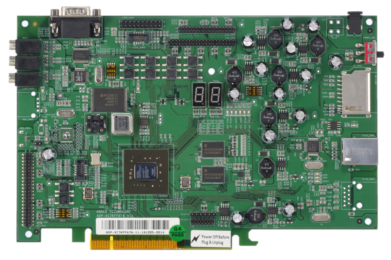
Figure 1 ADP-XC7K160

Figure 2 ADP-XC7K410
Feature Highlight
Feature
- Xilinx Kintex-7 FPGA XC7K160T/410T
- Encrypted Bitstream support
- 1 GB on-board DDR3*-800 SDRAM
- 128MB on-board NOR flash; 64MB for FPGA configuration, and 64MB for system storage
- 2MB SPI Flash
- 16KB I2C EEPROM
- 10/100 Ethernet RJ45 port
- DB9 UART port
- SD memory card slot
- IDE/GPIOs connector
- 10 and 20 pins AICE ports
- 8 user defined push buttons
- LCD module connector
- MIC-in, Line-in, and Line-out with AC97 audio codec
- Two 7-segment LED displays
*This feature requires Xilinx’s IP support
Development Tools and Platforms
- AndeSight™ version 2.0.0 or later
- AndeShape™ Board Support Package(BSP)
