TetraMem Integrates Energy-Efficient In-Memory Computing with Andes RISC-V Vector Processor

By Wenbo Yin, Vice President of IC Design, TetraMem Inc.

Introduction
The rapid proliferation of artificial intelligence (AI) across a growing number of hardware applications has driven an unprecedented demand for specialized compute acceleration not met by conventional von Neumann architectures. Among the competing alternatives, one showing the greatest promise is analog in-memory computing (IMC). Unleashing the potential of multi-level Resistive RAM (RRAM) is making the promise more real today than in the past. Leading this development, TetraMem, Inc., a Silicon Valley based startup, is addressing the fundamental challenges holding this solution back. The company’s unique IMC that employs multi-level RRAM technology provides more efficient, low-latency AI processing that meets the growing needs of modern applications in AR/VR, mobile, IoT, and beyond.

Background on the Semiconductor Industry
The semiconductor industry has seen significant advancements over the past few decades, particularly in response to the burgeoning needs of AI and machine learning (ML). Innovations in chip design have pushed the boundaries of performance and efficiency. However, several intrinsic persistent challenges remain, such as the von Neumann bottleneck and memory wall, which limits data transfer rates between the CPU and memory, and the escalating power consumption and thermal management issues associated with advanced node technologies.

In-memory computing (IMC) represents a ground-breaking computing paradigm shift in how data processing is accomplished. Traditional computing architectures separate memory and processing units, resulting in significant data transfer overheads, especially for the data centric AI applications. On the other hand, IMC integrates memory and processing within the same physical location, enabling faster and more efficient data computations with a crossbar array architecture to further eliminate the large quantity of intermediate data from those matrix operations. This approach is particularly beneficial for AI and ML applications, where large-scale data processing and real-time analytics are critical.

Selecting a suitable memory device for IMC is crucial. Traditional memory technologies like SRAM and DRAM are not optimized for in-memory operations due to their device and cell constraints and their volatility idiosyncrasies. RRAM, with its high density, multilevel capability and non-volatility with superior retention, overcomes these challenges with no refresh needed. The working principle of RRAM involves adjusting the resistance level of the memory cell through controlled voltage or current, mimicking the behavior of synapses in the human brain. This capability makes RRAM particularly suited for analog in-memory computing.

TetraMem has focused its efforts on multi-level RRAM (memristor) technology, which offers several advantages over traditional single level cell memory technologies. RRAM’s ability to store multiple bits per cell and perform efficient matrix multiplications in situ makes it an ideal candidate for IMC. This technology addresses many of the limitations of conventional digital computing, such as bandwidth constraints and power inefficiency.

The RRAM programmable circuit element remembers its last stable resistance level. This resistance level can be adjusted by applying voltage or current. Changes in magnitude and direction of voltage and current applied to the element alters its conductance, thus changing its resistivity. Akin to how a human neuron functions, this mechanism has diverse applications: memory, analog neuron, and, at TetraMem, in-memory computing. The operation of an RRAM is driven by ions. With control of the conductive filament size, ion concentration and height, different multi-levels for cell resistance can be precisely achieved.

Data processed in the same physical location as it is stored with minimum intermediate data movement and storage results in low power consumption. Massive parallel computing by crossbar array architecture with device-level grain cores yields high throughput. And computing by physical laws in this way (Ohm’s law and Kirchhoff’s current law) produces low latency. TetraMem’s nonvolatile compute in-memory cell reduces power consumption by orders of magnitude over a conventional digital von Neumann architecture.

Notable Achievements
TetraMem has achieved significant milestones in the development of RRAM technology. Notably, the company has demonstrated an unprecedented device with 11 bits per cell, achieving over 2,000 levels in a single element. This level of precision represents a major breakthrough in memory compute technology.

Recent publications in prestigious journals such as Nature1 and Science2 highlight TetraMem’s innovative approaches. Techniques to improve cell noise performance and to enhance multi-level IMC have been key areas of advancement. For example, TetraMem has developed proprietary algorithms to suppress random telegraph noise, resulting in superior memory retention and endurance characteristics for RRAM cells.

Operation of IMC
TetraMem’s IMC technology utilizes a crossbar architecture, where each cross-point in the array corresponds to a programmable RRAM memory cell. This configuration allows for highly parallel operations, which are essential for neural network computations. During a Vector-Matrix Multiplication (VMM) operation, input activations are applied to the crossbar array, and the resulting computations are collected on the bit lines. This method significantly reduces the need to transfer data between memory and processing units, thereby enhancing computational efficiency.

Real-World Applications
TetraMem’s first evaluation SoC through the commercial fab process, the MX100 chip (see figure) exemplifies the practical applications of its IMC technology. The chip has been demonstrated in various on-chip demos, showcasing its capabilities in real-world scenarios. One notable demo, the Pupil Center Net (PCN), illustrates the chip’s application in AR/VR for face tracking and authentication monitoring in autonomous vehicles.

To facilitate the adoption of its technology, TetraMem provides a comprehensive Software Development Kit (SDK). This SDK enables developers to define edge AI models seamlessly. Furthermore, the integration with Andes Technology Inc.’s NX27V RISC-V CPU with Vector extensions streamlines operations, making it easier for customers to deploy TetraMem’s solutions in their products.

The TetraMem IMC design is great for matrix multiplication but not as efficient in other functions such as vector or scalar operations. These operations are used frequently in neural networks.  For these functions, Andes provides the flexibility of a CPU plus a vector engine as well as an existing SoC reference design and a mature compiler and library to accelerate our time to market.

TetraMem collaborated with Andes Technology to integrate its IMC technology with Andes’ RISC-V CPU with Vector Extensions. This partnership enhances the overall system performance, providing a robust platform for a variety of AI tasks. The combined solution leverages the strengths of both companies, offering a flexible and high-performance architecture.

Looking ahead, TetraMem is poised to introduce the MX200 chip based on 22nm, which promises even greater performance and efficiency. This chip is designed for edge inference applications, offering low-power, low-latency AI processing. The MX200 is expected to open new market opportunities, particularly in battery-powered AI devices where energy efficiency is paramount.

Conclusion
TetraMem’s advancements in in-memory computing represent a significant leap forward in the field of AI hardware. By addressing the fundamental challenges of conventional computing, TetraMem is paving the way for more efficient and scalable AI solutions. As the company continues to innovate and collaborate with industry leaders like Andes Technology, the future of AI processing looks promising. TetraMem’s solution not only enhances performance but also lowers the barriers to entry for adopting cutting-edge AI technologies.

  1. “Thousands of conductance levels in memristors monolithically integrated on CMOS”, Nature, Mar 2023 https://rdcu.be/c8GWo
  2. “Programming memristor arrays with arbitrarily high precision for analog computing”, Science, Feb 2024 https://www.science.org/doi/10.1126/science.adi9405
Continue ReadingTetraMem Integrates Energy-Efficient In-Memory Computing with Andes RISC-V Vector Processor

Rivos Selects Andes NX45 for Control Functions in Upcoming High-Performance RISC-V SoC

NX45 Becomes the Only RISC-V Core to Pass Rivos’ Rigorous Verification Process After Extensive Evaluation of Leading RISC-V Cores

San Jose, CA – Sep. 11, 2024— Rivos Inc., a RISC-V Premier member company focused on accelerating data analytics and Generative AI workloads and Andes Technology, a leading supplier of 32/64-bit RISC-V processor cores and a RISC-V Founding Premier member , announced that Rivos Inc. has licensed the Andes NX45 RISC-V Processor for key control functions in their products.

Rivos was founded in 2021 by industry veterans from Google, Intel, Apple, and PA-Semi and has assembled a world class team of silicon, software, and platform engineers to build industry-leading power efficient, high performance, secure server solutions based on a high-end internally developed RISC-V CPU. 

To run control and scheduling for several key functions in Rivos’ SoC, the highly configurable and extensible Andes NX45 RISC-V processor was chosen because it allows the best tradeoffs in performance and efficiency, while meeting the highest quality standards.

“We are excited to welcome Rivos Inc. to the RISC-V community and wish them tremendous success,” said Dr. Charlie Su, President & CTO of Andes Technology. “We are proud that Rivos chose the NX45 for their project. Rivos’ selection of Andes is a testament to our flexibility, development rigor, and dedication to quality.”

“The growth of the RISC-V ecosystem and customer traction has been remarkable, and we are thrilled to be part of this movement,” said Belli Kuttanna, Co-Founder and CTO at Rivos Inc. “After evaluating several leading RISC-V cores, the Andes NX45 stood out as the only core that passed our proprietary verification process with zero bugs. Its robust configuration options and ease of integration made it the clear choice as our 64-bit control core.”

Rivos recently raised over $250M in an oversubscribed series A-3 funding round to enable the company to tape out its first silicon product, expand manufacturing operations, and scale platform hardware and software engineering efforts.

Andes Technology has been delivering a full range of processing solutions for over 19 years.  Launched in 2019, the AndesCore™ 45-series includes in-order 8-stage dual-issue RISC-V processors with options to support multicore, Linux, and vector processing to meet the demands of many high-end applications.  Andes’ customers benefit from a full-product offering including AndeSight™ IDE, Andes Custom Extension™ (ACE) and related software, and modeling, debug, and trace tools to accelerate their SoC development.

About Rivos Inc.
Rivos has assembled a world class team of silicon, software and platform designers implementing the long term vision of building industry-leading power efficient, high performance, secure server solutions, based on RISC-V, using workload-defined hardware. Rivos supports the intense requirements of the large language models and data analytics through a full solution of optimized chips; combining RISC-V CPUs, a Data Parallel Accelerator, and a reference multi-chip OCP modular server along with a full firmware-to-application open software stack. Rivos is hiring engineering talent across multiple disciplines.

About Andes Technology
Nineteen years in business and a Founding Premier member of RISC-V International, Andes is publicly-listed company (TWSE: 6533SIN: US03420C2089ISIN: US03420C1099) and a leading supplier of high-performance/low-power 32/64-bit embedded processor IP solutions, and the driving force in taking RISC-V mainstream. Its V5 RISC-V CPU families range from tiny 32-bit cores to advanced 64-bit Out-of-Order processors with DSP, FPU, Vector, Linux, superscalar, functional safety and/or multi/many-core capabilities. By the end of 2023, the cumulative volume of Andes-Embedded™ SoCs has surpassed 14 billion. For more information, please visit https://www.andestech.com. Follow Andes on LinkedInFacebookXBilibili  and YouTube


Continue ReadingRivos Selects Andes NX45 for Control Functions in Upcoming High-Performance RISC-V SoC

Resiltech and Andes Technology Announce Collaboration to Deliver Advanced STL Solutions for Andes Automotive-Grade RISC-V Processor IP

Pontedera, Italy and Hsinchu, TaiwanAug 29th, 2024 – Resiltech, a renowned provider of comprehensive security and safety solutions and services, and Andes Technology, a leading supplier of high-performance, low-power RISC-V processor IP are pleased to announce a strategic collaboration to deliver advanced Software Test Library (STL) solutions for Andes’ automotive-grade RISC-V processor IP.

This partnership combines Andes Technology’s expertise in delivering cutting-edge RISC-V processor IP with Resiltech’s proven track record in developing robust STL solutions. Together, they aim to enhance the safety and reliability of automotive electronic systems.

The collaboration will focus on enabling Resiltech to develop advanced STL that can perform safety diagnostic analysis against Andes automotive-grade processor IP line-up. The combined offerings from both companies ensure rigorous fault detection and mitigation, providing automotive OEMs and Tier-1 suppliers with reliable and safe processor solutions.

Resiltech’s STLs are designed to streamline the safety certification process of the target system providing a pre-certified product specifically tailored for the target silicon without the need of any additional activities, an easy and fast SW integration strategy and additional ad-hoc support for the system safety integration.

Andes is committed to delivering functionally safe automotive RISC-V IP, having achieved company-wide ISO-26262 ASIL-D compliance for systematic development process in 2020. Since then, Andes has released the 25-SE series processors, including the N25F-SE and D25F-SE, which have achieved ASIL-B full compliance and gained over a dozen customer projects.  Some customers have already entered mass production and also achieved SoC level ISO-26262 compliance leveraging Andes’ work products.  Furthermore, the company plans to release the D45-SE and D23-SE processors including ISO-26262 certification in the coming months, targeting ASIL-D full compliance.

“We are thrilled to partner with Resiltech to bring enhanced safety features to our automotive-grade RISC-V IP,” said Samuel Chiang, marketing director of Andes Technology. “This collaboration underscores our commitment to providing our customers with the most advanced and reliable solutions for automotive applications.”

Francesco Rossi, Safety Solution Director of Resiltech, added, “Our expertise in STL development complements Andes Technology’s innovative processor IP. Together, we are set to provide the automotive industry with a comprehensive solution that not only meets but exceeds the stringent safety requirements of modern vehicles.”

This collaboration marks a significant milestone in advancing the safety of automotive electronic systems, paving the way for the next generation of smart and safe vehicles.

About Andes Technology
Nineteen years in business and a Founding Premier member of RISC-V International, Andes is a publicly-listed company (TWSE: 6533SIN: US03420C2089ISIN: US03420C1099) and a leading supplier of high-performance/low-power 32/64-bit embedded processor IP solutions. Its V5 RISC-V CPU families range from tiny 32-bit cores to advanced 64-bit Out-of-Order processors with DSP, FPU, Vector, Linux, superscalar, automotive and/or multi/many-core capabilities. By the end of 2023, the cumulative volume of Andes-Embedded™ SoCs has surpassed 14 billion. For more information, please visit https://www.andestech.com . Follow Andes on LinkedInTwitterBilibili and YouTube!

About Resiltech
ResilTech is a company providing state-of-the-art solutions and services in safety and security with its 15+ years of experience gained supporting customers operating in Critical Systems. In addition, the company integrates industrial expertise with research and development skills developed while constantly joining, since its foundation, national and international R&D projects. The company is a worldwide leading provider of Software Test Libraries (STLs) for a variety of processing nodes and it is now positioning itself as the reference provider of STLs for the RISC-V ecosystem. For more information, please visit http://www.resiltech.com.

Continue ReadingResiltech and Andes Technology Announce Collaboration to Deliver Advanced STL Solutions for Andes Automotive-Grade RISC-V Processor IP

TASKING宣布为Andes晶心科技提供符合ASIL功能安全(FuSa)标准的汽车 RISC-V IP的编译程序支持

使SoC设计团队和汽车软件开发人员能够建立优化且可认证的软件解决方案。

德国慕尼黑 – 2024年8月19日 – TASKING 很荣幸地宣布其符合ISO 26262(功能安全)和ISO/SAE 21434(网络安全)标准的编译程序,现已完全支持Andes晶心通过功能安全(FuSa)认证的RISC-V IP。这一进展扩展了TASKING涵盖编译、除错、效能调校、时序与覆盖分析工具的RISC-V工具套件,为汽车系统开发提供了全面的解决方案。

这一里程碑在帮助SoC设计团队和汽车软件开发人员打造高度优化且基于可认证的RISC-V解决方案方面,取得了重大进展。新推出的RISC-V编译程序符合ASIL-D标准,无缝支持已通过和即将通过功能安全(FuSa)认证的Andes晶心RISC-V核心。值得注意的是,该编译程序能够适应RISC-V ISA及其扩展,包括Andes晶心特定的扩展(Andes-specific extensions),确保针对目标设备进行动态优化,从而提升效率和性能。

Andes晶心科技于2022年推出了全球首款完全符合ISO-26262标准的RISC-V核心N25F-SE,在汽车市场上取得了非凡的里程碑。接着,Andes晶心推出经ASIL-B认证的D25F-SE,配备RISC-V SIMD/DSP P-extension (draft)支持,可在单指令中高效处理多个数据。展望未来,Andes晶心科技将推出符合ASIL-D标准的处理器,包括精简且安全的D23-SE、高性能的D45-SE以及适用于ADAS应用的AX60系列核心。这些进展彰显了Andes晶心为多样化的汽车应用提供客制化解决方案的能力,凸显了其在汽车RISC-V IP市场的领先专业知识。

「AndesCore® RISC-V IP已通过ISO 26262认证,提供了可靠的汽车处理器解决方案组合,为芯片开发提供无与伦比的灵活性和效率优势。」Andes晶心科技市场处副处长姜新雨表示。「我们与TASKING的合作使汽车行业的客户能够加快开发进程,增强RISC-V安全关键应用的效能和稳健性。」

谈到这次合作,TASKING的RISC-V负责人Gerard Vink热情的表示:「我们很高兴能与Andes晶心科技及其生态系伙伴合作。我们的工具与Andes晶心RISC-V IP从虚拟原型到芯片实现的开发平台上之无缝互操作性,突显了我们为SoC开发团队提供全面生命周期支持的承诺。利用TASKING先进的功能安全(FuSa)和网络安全流程,我们的用户可以加快合规工作,加速基于 RISC-V 的汽车软件解决方案的上市时间。」

关于Andes晶心科技
Andes晶心科技股份有限公司于2005年成立于新竹科学园区,2017年于台湾证交所上市 (TWSE: 6533SIN: US03420C2089ISIN: US03420C1099)。Andes晶心是RISC-V国际协会的创始首席会员,也是第一家推出商用RISC-V向量处理器的主流CPU供货商。为满足当今电子设备的严格要求,Andes晶心提供可配置性高的32/64位高效能CPU核,包含DSP、FPU、Vector、超纯量  (Superscalar)、乱序执行  (Out-of-Order)、多核心及车用系列,可应用于各式SoC与应用场景。Andes晶心提供功能齐全的整合开发环境和全面的软/硬件解决方案,可帮助客户在短时间内创新其SoC设计。截至2023年底,Andes-Embedded™ SoC累计出货量已超过140亿颗。 更多关于Andes晶心的信息,请参阅晶心官网https://www.andestech.com 。订阅Andes晶心微信公众号AndesTech及Bilibili获得最新消息!


关于TASKING
TASKING是一家总部位于德国慕尼黑的领先开发工具供货商,为多核心架构提供高效能、高质量、以安全和保障为导向的嵌入式软件开发工具。
汽车制造商和供货商以及世界各地的邻近市场都使用TASKING的开发工具来实现安全关键领域的高性能应用。
TASKING的嵌入式软件开发解决方案为您的整个软件开发过程提供业界领先的生态系统。每款TASKING编译程序都针对特定架构设计并满足您所在行业,包括汽车、工业、电信和数据通讯的特定要求。
作为高质量、功能和安全兼容的嵌入式软件开发工具领域公认的领导者,TASKING 使您能够透过针对业界领先的微处理器和微控制器的编译程序、调试程序和RTOS支持来建立具有一流大小和性能的程序代码。
自2021年2月以来,TASKING的大部分股份由金融投资者FSN Capital拥有,该投资者在成功进行业务拆分后,将集团置于长期增长轨道上。欲了解更多信息,请访问 www.tasking.com 或在 LinkedIn 上追踪我们:https://www.linkedin.com/company/tasking-inc

Continue ReadingTASKING宣布为Andes晶心科技提供符合ASIL功能安全(FuSa)标准的汽车 RISC-V IP的编译程序支持

Andes晶心科技与Arteris合作加速RISC-V SoC的采用

重点:
– Andes晶心科技与 Arteris 的合作旨在支持共同客户更多地采用 RISC-V SoC。
– 重点关注: 消费类电子、通讯、工业应用和人工智能等广泛市场的高性能/低功耗RISC-V设计。
– 此次合作展示了Andes晶心领先的RISC-V处理器IP和Arteris互连IP于芯片中整合优化的解决方案。

加利福尼亚州坎贝尔 – 2024 年 8 月 15 日 – 专注于加速系统单芯片(SoC)创建的领先系统IP提供商Arteris (Nasdaq: AIP),与高效率、低功耗、32/64 位 RISC-V 处理器核心的领先供货商和 RISC-V 国际协会创始首席成员Andes晶心科技(TWSE: 6533),今天宣布双方建立合作伙伴关系,共同推动在人工智能、5G、网络、电信、存储、AIoT和太空应用领域中基于 RISC-V 的 SoC设计创新。

Andes晶心QiLai RISC-V平台是配备QiLai SoC的开发板,采用Andes晶心RISC-V处理器IP以及用于芯片上网络连接的Arteris FlexNoC互连IP。QiLai SoC整合了2.2 GHz的64位Andes晶心AX45MP多核处理器(四核集群)和1.5 GHz的NX27V向量处理器,使用Arteris的芯片上网络(NoC)互连IP,并包含PCIe、DDR、SRAM和通用I/O的子系统,这些子系统使用AMBA AXI协议,支持软件包括OpenSUSE Linux发行版、AndeSight™工具链、AndeSoft™软件栈(software stacks)和用于将AI/ML模型转换为可执行文件的AndesAIRE™ NN SDK。

「尽管AndesCore® AX45MP和NX27V处理器已被广泛使用,我们仍然很高兴看到QiLai SoC在新项目上能成功。」Andes晶心科技总经理暨技术长苏泓萌博士表示。「Arteris NoC IP是QiLai SoC中实现灵活、高性能、高阶层连接(top-level connectivity)的最佳选择。QiLai平台增强了RISC-V软件的快速开发和评估,加速了RISC-V生态系统的扩展。」

「我们很高兴能与Andes晶心科技合作,支持QiLai平台的互操作性,进一步加速RISC-V技术被主流应用采用。」Arteris首席营销长Michal Siwinski表示。「我们的合作支持我们成为SoC的创新推动力,使我们的共同客户能够高效地专注于实现未来的创新突破。」

Arteris的非缓存一致性FlexNoC NoC IP和缓存一致性Ncore NoC IP提供可扩展、低延迟和高能效的芯片内通信,从而在复杂的 SoC 设计中实现卓越的性能。这项技术促进了高性能、低功耗CPU IP的整合,增强系统功能和互操作性,尤其是在快速增长的RISC-V生态系统中。这种可配置和适应性强的互联解决方案可与各种组件无缝连接,以降低风险并加速上市时间。透过连接经过充分测试的CPU IP模块,系统设计师可以利用Arteris的NoC IP来提升下一代SoC的可靠性和质量。

客户可以透过电子邮件 sales@andestech.com 向Andes晶心科技申请包含Andes QiLai RISC-V平台的开发工具包。有关合作伙伴关系和各自产品的更多信息,请联系  info@arteris.cominfo@andestech.com


关于Arteris
Arteris是当今电子系统中加速系统单芯片(SoC)开发的领先系统IP供货商。Arteris的片上网络(NoC)互连IP和SoC整合自动化技术可实现更高的产品效能、更低的功耗和更快的上市时间,提供更好的SoC经济效益,使其客户可以专注于构思下一步的创新。了解更多信息,请访问 arteris.com

关于Andes晶心科技
Andes晶心科技股份有限公司于2005年成立于新竹科学园区,2017年于台湾证交所上市 (TWSE: 6533SIN: US03420C2089ISIN: US03420C1099) 。Andes晶心是RISC-V国际协会的创始首席会员,也是第一家推出商用RISC-V向量处理器的主流CPU供货商。为满足当今电子设备的严格要求,晶心提供可配置性高的32/64位高效能CPU核心,包含DSP、FPU、Vector、超纯量 (Superscalar)、乱序执行 (Out-of-Order)、多核心及车用系列,可应用于各式SoC与应用场景。Andes晶心提供功能齐全的整合开发环境和全面的软/硬件解决方案,可帮助客户在短时间内创新其SoC设计。截至2023年底,Andes-Embedded™ SoC累计出货量已超过140亿颗。 更多关于Andes晶心的信息,请浏览Andes晶心官网 https://www.andestech.com。订阅Andes晶心微信公众号AndesTech及Bilibili 获得最新消息!

© 2004-2024 Arteris, Inc. All rights reserved worldwide. Arteris, Arteris IP, the Arteris IP logo, and the other Arteris marks found at https://www.arteris.com/trademarks are trademarks or registered trademarks of Arteris, Inc. or its subsidiaries. All other trademarks are the property of their respective owners.

Continue ReadingAndes晶心科技与Arteris合作加速RISC-V SoC的采用

Rain AI宣布Andes 晶心科技成为其RISC-V合作伙伴

Rain AI取得采用Andes 晶心科技AX45MPV的授权,并与Andes 晶心客制运算事业部合作,加速推出革命性的存内计算(CIM)生成式人工智能解决方案

【美国旧金山】— 202481日—高效能低功耗32/64位RISC-V处理器核心领导供货商暨RISC-V国际协会创始首席会员Andes 晶心科技(TWSE: 6533)今日宣布向存内计算(CIM)技术的先驱者Rain AI授权使用Andes 晶心RISC-V向量处理器AX45MPV。Rain AI设计了新颖的加速器解决方案,且双方正在合作并加速推进Rain AI产品开发。

随着全球经济大量采用生成式人工智能为消费者及企业提供前所未有的利益,无论是应用在云端、边缘,或特别是在最小的传感器中,能量消耗是一大挑战。存内计算(CIM)是目前降低能耗最具潜力的解决方案,可将能耗降低多达50倍。透通过直接在内存单元中执行计算,CIM可以显著减少机器学习中常见矩阵运算所需的能量。

然而,仅凭CIM本身无法完全解决大量且不断增长的机器学习运算需求。RISC-V CPU为基于CIM基础的NPU提供高效编程且未来看好的理想处理器选择,RISC-V架构允许用户能够添加客制指令来呼叫CIM计算模块,从而减轻软件开发的负担。Andes 晶心科技为此特别提供了COPILOT编译程序来自动客制化指令。

Andes 晶心科技董事长暨执行长林志明表示:「Andes 晶心科技非常荣幸且兴奋地与Rain AI成为授权及合作伙伴关系。作为首家RISC-V向量处理器供货商,我们认为CIM是实现生成式AI应用的必要技术,因此,我们专注于支持CIM客户。据我们所知,Rain AI采用数字CIM技术设计了最节能的矩阵乘法单元,因此我们期待Rain AI 在未来发布突破性的解决方案。」

Rain AI执行长William Passo对此表示赞同,并说道:「很少能遇到与我们在市场及技术愿景上有着共同理解的供货商,Andes 晶心不仅提供了最优秀的RISC-V解决方案来满足我们的技术需求,还愿意投入资源帮助我们加速开发产品,并成功降低人工智能运算所需的能源消耗。将最先进的模型在任何外型尺寸的设备中运行是人工智能的未来,与Andes 晶心的合作让我们更向此迈进了一大步。」

事实上,Rain AI进一步与Andes 晶心客制运算事业部(CCBU)合作,通过现场及远程咨询服务,协助加速集成Andes 晶心AX45MPV和ACE/COPILOT客制指令。Andes 晶心客制运算事业部(CCBU)是一支由专家组成的小团队,负责为一些具有领先技术的授权客户进行复杂的客制及集成工作。

两家公司可以共同分享AX45MPV和Andes 晶心独特的RISC-V客制指令技术ACE/COPILOT的独到之处。ACE/COPILOT在补充Rain AI开创性的CIM硬件、编译程序和软件中发挥了至关重要的作用,提供可扩展的机器学习(ML)解决方案,适用于多种部署形式。Rain AI将在2025年初,发表其加速器解决方案。

关于Andes 晶心Andes Technology)
Andes晶心科技股份有限公司于2005年成立于新竹科学园区,2017年于台湾证交所上市 (TWSE: 6533; SIN: US03420C2089; ISIN: US03420C1099)。Andes晶心是RISC-V国际协会的创始首席会员,也是第一家推出商用RISC-V向量处理器的主流CPU供货商。为满足当今电子设备的严格要求,Andes晶心提供可配置性高的32/64位高效能CPU核,包含DSP、FPU、Vector、超纯量  (Superscalar)、乱序执行  (Out-of-Order)、多核心及车用系列,可应用于各式SoC与应用场景。Andes晶心提供功能齐全的整合开发环境和全面的软/硬件解决方案,可帮助客户在短时间内创新其SoC设计。截至2023年底,Andes-Embedded™ SoC累计出货量已超过140亿颗。 更多关于Andes晶心的信息,请参阅晶心官网https://www.andestech.com 。订阅Andes晶心微信公众号AndesTech及Bilibili获得最新消息!

关于RAIN AI
Rain AI的使命是通过打造全球最高效能的AI硬件,促进大量且先进人工智能技术的普及。它利用创新的存内计算(CIM)技术、RISC-V处理器核、先进的封装技术和优化的机器学习算法,为生成式AI推理和训练提供了灵活的解决方案。藉由领先的AI模型共同设计硬件,Rain AI在AI效率及效能方面开创了新的标准。Rain AI的投资者包含Sam Altman、Dan Gross以及Y Combinator。如需了解详情,请参阅http://www.rain.ai

Continue ReadingRain AI宣布Andes 晶心科技成为其RISC-V合作伙伴

Andes晶心科技加入甲辰计划,共建 RISC-V 生态繁荣

高效能、低功耗、32/64 RISC-V处理器核的领先供货商Andes晶心科技正式加入甲辰计划,致力于在下一个丙辰年(2036龙年)之前,基于 RISC-V 实现从数据中心到桌面办公、从移动穿戴到智能物联网全信息产业覆盖的开放标准体系及开源系统软件栈,使RISC-V软硬件生态到作为主流指令集架构所需的生态成熟度。

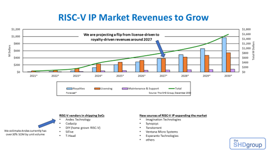
Andes晶心科技成立于2005年,是RISC-V国际协会的创始首席成员。截至2023年底,搭载AndesCore®的SoC累计出货量已达140亿颗。根据2024年1月发布的SHD营销报告 (SHD 2024 RISC-V Market Analysis),Andes晶心科技在RISC-V IP供应商中市场占有率高达30%,位居全球第一。

在过去两年内,晶心科技陆续推出了一系列全新的RISC-V处理器,引领着包括人工智能、车载应用、多媒体处理以及物联网领域的产业创新。这些处理器包括市场上首个超过1024比特的RISC-V向量处理器AndesCore® AX45MPV,以及场上第一个完全符合ISO 26262标准的车规核N25F-SE,和D25F-SE。此外还有高性能超标量乱序多核处理器AX65,以及支持多项RISC-V最新指令及安全架构的小型处理器D23。

此外,Andes还推出了AI产品线AndesAIRE™(Andes AI Runs Everywhere),以DSP处理器(像D23和D25),向量处理器(像NX27V和AX45MPV)和硬件加速器AnDLA为基础,为边缘和端侧推理提供全面的硬件和软件人工智能整合解决方案。Andes晶心科技将推出更为全面的产品线,进一步满足不断增长的市场需求。

甲辰计划(RISC-V Prosperity 2036诞生于2024年除夕,由大陸国内多家 RISC-V 软件及芯片团队联合发起,并已经吸引数十家国内外从事 RISC-V 产品及软件开发的企业加入。我们相信RISC-V 生态正在进入前所未有的爆炸式增长的初期阶段:在2025年,RISC-V或将迎来预计超过100万名RISC-V应用开发者,与此同时RISC-V将在2025年进入世界超算TOP500、并在2030年进入TOP10。我们正处于一个计算机体系架构和基础软件系统的黄金时代,开放指令集架构带来了大量新的科学问题和工程挑战。

作为全球领先的RISC-V生态贡献团队及个人,我们邀请志同道合者联合起来,以龙年为起点开启加速历程,为实现本计划的愿景和使命而并肩奋斗。让我们用一纪的时间,在所有基础关键行业领域完成面向RISC-V的适配与优化,并形成超过壹万人的顶尖人才网络。

关于晶心科技(Andes Technology
Andes晶心科技股份有限公司于2005年成立于新竹科学园区,2017年于台湾证交所上市 (TWSE: 6533 SIN: US03420C2089ISIN: US03420C1099)Andes晶心是RISC-V国际协会的创始首席会员,也是第一家推出商用RISC-V向量处理器的主流CPU供货商。为满足当今电子设备的严格要求,Andes晶心提供可配置性高的32/64位高效能CPU核,包含DSPFPUVector、超纯量 (Superscalar)、乱序执行 (Out-of-Order)、多核及车用系列,可应用于各式SoC与应用场景。Andes晶心并提供功能齐全的整合开发环境和全面的软/硬件解决方案,可说明客户在短时间内创新其SoC设计。截至2023年底,嵌入AndesCore® SoC累积总出货量已达140亿颗。更多关于Andes晶心的信息,请参阅晶心官网https://www.andestech.com。订阅晶心微信公众号AndesTechBilibili获得最新消息!

Continue ReadingAndes晶心科技加入甲辰计划,共建 RISC-V 生态繁荣

Andes 晶心科技宣布推出QiLai系统芯片和Voyager开发板

2024年7月24日— 高效能低功耗32/64位RISC-V处理器核心领导供货商暨RISC-V国际协会创始首席会员Andes 晶心科技(TWSE: 6533)今日宣布推出QiLai (奇莱)系统芯片(SoC)和Voyager开发板,以进一步加速大规模RISC-V应用的开发和移植。

QiLai系统芯片内建高效能四核心RISC-V AX45MP的集群和一颗NX27V向量处理器。超纯量多核心处理器AndesCore® AX45MP搭载2MB二级高速缓存以及处理一二级缓存一致性的管理机制(coherence manger),以及用于Linux应用的内存管理单元(MMU)。而向量处理器AndesCore® NX27V具备512KB的数据缓存,能支持完整的RISC-V标准数据类型以及晶心为AI应用优化的延伸数据类型。NX27V包含高效能的纯量单元及一个乱序向量处理单元(VPU),其向量长度(VLEN)及数据信道宽度(DLEN)皆为 512 位,每个周期最多能产生四个 512 位的运算结果。NX27V与AX45MP集群相互合作,将QiLai打造为异质软件开发平台,使对称式多核心Linux操作系统 (SMP),实时操作系统 (RTOS )或裸机 (bare metal)系统能够在此平台上同时运行。AX45MP和NX27V的最高运行频率分别为2.2 GHz和1.5 GHz,而QiLai在全速运行时的总功耗约为5瓦。

Voyager是一款符合 9.6” x 9.6” Micro ATX硬件尺寸的开发板,内含QiLai系统芯片、16GB DDR4 SIMM插槽、JTAG调试器、USB到UART网桥、I2S音频编译码器、16Mb SPI Flash启动程序代码、SD卡插槽,以及多个可用于连接GPU卡和 SSD等多种外部设备的PCIe Gen4插槽。其支持软件涵盖OpenSUSE Linux发行版、AndeSight™ 工具链、AndeSoft™ 软件堆栈和AndesAIRE™ NN SDK,用于将 AI/ML模型转换为在NX27V向量处理器上运行的可执行文件。

「我们很高兴地宣布QiLai系统芯片的推出,其整合了广受采用的 AndesCore® AX45MP多核心和NX27V向量处理器。」Andes 晶心科技董事长暨执行长林志明表示。「尽管这两款处理器已被多位客户授权并经过量产芯片的验证,我们仍然很高兴看到它们在晶心自家的芯片上首次运行。采用台积电先进的7纳米制程技术制造,QiLai系统芯片和其Voyager开发板充分展现了晶心为支持快速RISC-V软件开发的承诺。Andes 晶心科技将继续专注于IP供应,不涉足芯片业务,而此项目是为了提供更好的处理器IP评估和应用开发,也是晶心在2021年GDR募资后的优秀成果。」、「若有芯片公司对此一芯片的进入量产有兴趣,Andes 晶心科技亦可考虑以特殊商务授权模式,让芯片公司有机会取得授权,将QiLai芯片带进量产。」

「Andes 晶心科技接收过许多来自合作伙伴和软件开发者的需求,希望能提供基于芯片的平台,使他们能更有效率地为RISC-V开发软件。」Andes 晶心科技总经理暨技术长苏泓萌博士指出。「搭载QiLai系统芯片的Voyager开发板是我们对该需求的响应,亦是实现快速开发和评估多种RISC-V软件的重要一步,并同时有助于扩展RISC-V生态系统。」

关于Andes 晶心科技 (Andes Technology)
Andes 晶心科技股份有限公司于2005年成立于新竹科学园区,2017年于台湾证交所上市 (TWSE: 6533 SIN: US03420C2089ISIN: US03420C1099)。晶心是RISC-V国际协会的创始首席会员,也是第一家推出商用RISC-V向量处理器的主流CPU供货商。为满足当今电子设备的严格要求,晶心提供可配置性高的32/64位高效能CPU核心,包含DSP、FPU、Vector、超纯量  (Superscalar)、乱序执行  (Out-of-Order)、多核心及车用系列,可应用于各式SoC与应用场景。晶心并提供功能齐全的整合开发环境和全面的软/硬件解决方案,可帮助客户在短时间内创新其SoC设计。截至2023年底,Andes-Embedded™ SoC累计出货量已超过140亿颗。 欲了解更多信息,请访问https://www.andestech.com 。请立即透过LinkedInXBilibili以及YouTube追踪晶心最新消息。

Continue ReadingAndes 晶心科技宣布推出QiLai系统芯片和Voyager开发板

Andes晶心科技与 MachineWare 合作AndesCore® AX45MPV的仿真器供用户可早期开发RISC-V软件

德国亚琛与台湾新竹 2024年7月18 MachineWare GmbH 与高效能低功耗32/64RISC-V处理器核心领导供货商同时也是RISC-V 国际协会创始首席会员的Andes晶心科技TWSE:6533),共同宣布了一个令人振奋的新合作篇章标志着战略合作伙伴关系的正式开始。这次合作针对的是极具创新性的AndesCore® AX45MPV,一款专为AI工作负载加速和应用层面设计的尖端多核RISC-V向量处理器。在此次合作中,MachineWare AX45MPV 无缝整合到其高效能模拟解决方案SIM-V中来并提供支持。事实证明,对于软件开发人员来说,这种解决方案能够有效地处理复杂的 AI Linux 堆栈相关工作。在芯片试产之前,使用该虚拟平台就可以简化软件开发、测试和验证。这次合作凸显了MachineWareAndes晶心科技在推动处理器技术进步方面的共同承诺。

SIM-VMachineWare的一项产品,对于RISC-V领域的开发人员来说,具有极大的价值。借助SIM-V,开发人员可以在首批芯片从晶圆厂回来之前,就彻底测试和验证其基于RISC-V的系统和软件应用。SIM-V 的核心是提供支持所有 RISC-V 标准扩充的快速指令集仿真器 (ISS)SIM-V的一大亮点是其方便使用的可自定义扩充性。透过简单的扩充SDK,开发人员可以快速整合自定义指令、寄存器和其他元素到仿真器中,以获得有关其设计选择的实时回馈。而使SIM-V真正与众不同的是其与SystemC TLM-2.0的整合。这一独特组合让用户能够将其IP模型无缝导入完整的系统仿真环境,提升平台的多功能性。

AX45MPV是一个648级流水线双发射多核心RISC-V处理器,包含RISC-V GCBP**P扩展指令集为草稿版本)扩展指令集功能,并支持具有内存管理单元
MMU)的对称多处理(SMP Linux,且最多可支持48位的虚拟地址。此外,它可以配置最多八个核心,并在一个cluster中配置带有缓存一致性管理器和最多8MB共享L2缓存的内存。AX45MPV的向量处理单元(VPU)实现了RISC-V向量扩展(RVV1.0版本,支持最多1024位向量宽度(VLEN)和数据信道宽度(DLEN)的配置。AX45MPV在处理大数据数组计算方面表现卓越,适用于计算机视觉、数字信号处理、图像处理、机器/深度学习和科学计算等应用。

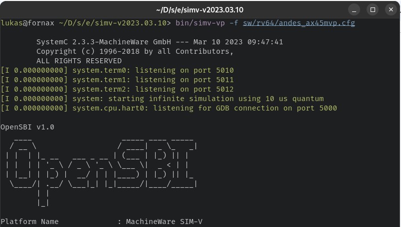
Figure 1: Invoking SIM-V with the AX45MPV configuration.

「我们非常高兴能与Andes晶心科技合作,在SIM-V中支持AX45MPV处理器。」MachineWare总经理Lukas Jünger表示。「与AX45MPV模型的整合使我们的共同客户能够在短时间内开发RISC-V LinuxAI软件堆栈software stacks并验证其功能。这将降低错误并提升软件质量,同时加速整体开发过程。」

Andes晶心科技与 MachineWare 的合作,展现了我们持续扩展 RISC-V 生态系统的决心,也就是让高效能模拟工具的采用更加便捷。」
Andes晶心科技市场处副处长姜新雨表示。「我们很高兴能与MachineWare携手推动RISC-V生态系统的扩展。我们相信RISC-V的指令集架构将促进创新,并有潜力改变人工智能市场。」


关于 MachineWare

MachineWare2022年成立于德国亚琛,拥有数十年系统级仿真和高性能仿真工具的经验。详情请访问官方网站
https://www.machineware.de/


关于Andes晶心科技

Andes晶心科技股份有限公司于2005年成立于新竹科学园区,2017年于台湾证交所上市 (TWSE: 6533; SIN: US03420C2089; ISIN: US03420C1099)。晶心是RISC-V国际协会的创始首席会员,也是第一家推出商用RISC-V向量处理器的主流CPU供货商。为满足当今电子设备的严格要求,晶心提供可配置性高的32/64位高效能CPU核心,包含DSPFPUVector、超纯量  (Superscalar)、乱序执行  (Out-of-Order)、多核心及车用系列,可应用于各式SoC与应用场景。晶心提供功能齐全的整合开发环境和全面的软/硬件解决方案,可帮助客户在短时间内创新其SoC设计。截至2023年底,Andes-Embedded SoC累计出货量已超过140亿颗。 更多关于Andes晶心的信息,请参阅晶心官网https://www.andestech.com 。订阅晶心微信公众号AndesTechBilibili获得最新消息!。


关于 RISC-V

RISC-V开放架构指令集架构由RISC-V International管理。详情请访问官方网站 https://riscv.org


MachineWare
联系窗口

Lukas Jünger, Managing Director

E-mail: lukas@mwa.re

Andes晶心科技联系窗口

Jonah McLeod, Press Contact, Andes Technology

Tel:
+1-510-449-8634

E-mail:
Jonahm@andestech.com


Continue ReadingAndes晶心科技与 MachineWare 合作AndesCore® AX45MPV的仿真器供用户可早期开发RISC-V软件

Andes晶心、经纬恒润暨先楫半导体三方携手 共筑RISC-V AUTOSAR软件生态

【2024年5月14日】Andes晶心科技、经纬恒润、先楫半导体联合宣布三方将开展合作,结合AndesCoreTM RISC-V处理器系列、先楫半导体HPM6200全线产品和经纬恒润的Vehicle OS软件平台解决方案,共同致力于RISC-V在车规级芯片领域的生态。此次合作经纬恒润AUTOSAR产品INTEWORK-EAS将适配先楫半导体HPM6200全线产品,对MCAL软件适配和工程集成进行支持,协助先楫半导体构建AUTOSAR解决方案。经纬恒润是目前少有的具备多款RISC-V车规级芯片适配经验的AUTOSAR基础软件供应商,长久以来积极推动生态共建,愿助力共同促进RISC-V车规级芯片生态繁荣。HPM6200全线产品共有12个产品型号,内置晶心科技AndesCoreTM D45单核或双核RISC-V处理器,该系列产品具有高性能、即时特性,应用领域包括新能源、储能、工业自动化、电动车等。通过本次合作,先楫半导体的芯片产品将以功能更加完善、服务更加完整的状态面向汽车电子不同应用场景,推动RISC-V技术在汽车电子领域的生态兼容。未来,经纬恒润与先楫半导体将保持合作,持续为迭代的新产品提供软件平台解决方案。

INTEWORK-EAS是经纬恒润自主研发,符合 AUTOSAR 标准的软件产品, 具备完整的 AUTOSAR 工具链,兼容多种业内主流数据格式,如 DBC、LDF、PDX、ODX、ARXML 等,支持与第三方 MCAL 工具链无缝集成。解决方案涵盖了嵌入式标准软件、AUTOSAR 工具链、集成服务和培训等各个方面的内容,旨在为OEM 和供应商提供稳定可靠、便捷易用的 AUTOSAR 平台。经纬恒润重视软硬件一体解决方案建设,自INTEWORK-EAS系列产品在国际知名芯片上经过广泛量产验证之后,经纬恒润不断深化与芯片企业之间的合作,共同向车规级市场提供更加完善的软硬件一体解决方案。对于经纬恒润而言,此次与先楫半导体HPM6200产品适配合作,将为其芯片生态合作圈增加新的重要成员,并使其保持在RISC-V生态适配方面的领先地位。

先楫半导体HPM6200采用晶心科技D45内核,循序执行8级双发射超纯量技术,具有优化的存储流水线设计以及进阶分支预测功能,主频达到 600 MHz,性能超过 3390 CoreMark和 1710 DMIPS, 同时支持符合IEEE754的单/双精度浮点运算单元(FPU)及RISC-V P (草案) 扩充指令 (DSP/SIMD)。D45系列核心也具有区域内存(local memory)支持的储存子系统,以及可配置的指令及资料快取记忆体,对于HPM6000系列支持大量记忆体的SoC,可进一步提升其软件效能。在应用市场而言, D45核心非常适合用于对响应时间和即时准确性特别要求的嵌入式应用产品。

HPM6200产品除了高算力RISC-V CPU,还整合一系列高性能外设以及外扩存储。此外, HPM6200 系列还提供增强 PWM 控制系统,以及用于复杂信号生成的可编程逻辑阵列PLA。集成了AES-128/256、SHA-1/256 加速引擎和硬件密钥管理器, HPM6200可以支持固件软件签名认证、加密启动和加密执行,可防止非法的代码替换、篡改或复制,进一步提升安全性。先楫半导体已完成ISO9001质量管理认证,和ISO 26262功能安全管理体系ASIL D认证,HPM6200 全线产品则通过AEC-Q100 G1认证,工作温度范围在-40~125℃。HPM6200与经纬恒润AUTOSAR适配之后,  将结合此软件方案全力推广于中国乃至全球的汽车市场。

经纬恒润嵌入式软件版块负责人张贺伟表示:「我们很高兴与晶心科技和先楫半导体合作,三方联合打造基于RISC-V的软硬件一体化方案,一同为国产化芯片生态建设推动前行。这个时代芯片快速迭代,正是发挥AUTOSAR中间件优势的时候,我们的芯片适配能力乐于接受新硬件环境的挑战,此次合作将再次证明这一点。未来,我们希望能够和更多的合作伙伴一起提供集成化解决方案,促进汽车产业向未来发展。」

先楫半导体执行长曾劲涛表示:「晶心科技D45处理器能够为先楫半导体超高速即时运算要求的MCU系列产品提供高效支持。在某些测试环境下,Andes CPU性能超越其他竞品,表现优异,且经由晶心产品导入所提供的即时技术支持,协助我们成功并快速地完成HPM6000系列的成功流片,双方团队可谓完美地进行了一次紧密高效的合作。」「对于先楫半导体来说, 此次适配经纬恒润的AUTOSAR合作,这不仅意味着先楫半导体产品得到了业界的广泛认可,更意味着内嵌Andes RISC-V内核的高性能微控制器产品在新能源电动汽车领域的应用前景得到了进一步拓展。」

晶心科总经理暨技术长苏泓萌博士表示:「晶心科技D45配合先楫半导体为开发者提供完备的生态系统, 客户得以设计出更高效能、和更多功能的软体,因而得以领先同业推出内嵌高效能RISC-V内核之MCU安全解决方案,此充分展现其团队的超高效率及卓越的研发能力。」「经纬恒润与先楫半导体的合作为行业树立了典范,也为后续的合作提供了宝贵经验。我们期待未来能够看到更多类似的合作,共同推动汽车电子产业的繁荣发展。」


关于经纬恒润 (HiRain Technology)
经纬恒润成立于2003年,专注于为汽车、无人运输等领域的客户提供电子产品、研发服务和高级别智能驾驶整体解决方案。总部位于北京,并在天津、南通、马来西亚有研发中心和现代化工厂,形成了完善的研发、生产、营销、服务体系。本着「价值创新、服务客户」的理念,公司坚持 「专业聚焦」、「技术领先」和「平台化发展」的战略,致力于成为国际一流综合型的电子系统科技服务商、智能网联汽车全栈式解决方案供应商,以及高级别智能驾驶MaaS解决方案领导者。经纬恒润是目前少数能够实现覆盖智能驾驶电子产品、研发服务及解决方案之全栈式解决方案的供应商。未来,经纬恒润将紧跟汽车行业发展大势,坚持自主创新,努力为国内外客户提供优质的产品和服务,为汽车行业的发展贡献自己的一份力量。更多关于经纬恒润的资讯,请访问https://www.hirain.com/

关于先楫半导体 (HPMicro Semiconductor)
先楫半导体是一家致力于高性能嵌入式解决方案的半导体公司,产品覆盖微控制器、微处理器和周边芯片,以及配套的开发工具和生态系统。 公司成立于2020年6月,总部坐落于上海市张江高科技园区,幷在天津、深圳、苏州和杭州均设立分公司。 核心团队来自世界知名半导体公司管理团队,具有15年以上且超过20个SoC丰富的研发及管理经验。先楫半导体以产品质量为本,所有产品均通过严格的可靠性测试。目前已经量产的高性能通用MCU产品系列包含HPM6700/6400、HPM6300、HPM6200、HPM5300及HPM6800,性能领先国际同类产品幷通过AEC-Q100认证。公司已完成ISO9001质量管理认证和ISO 26262/IEC61508功能安全管理体系双认证,全力服务中國工业、汽车和新能源市场。先楫半导体将与世界知名晶圆厂、封装测试厂及其它战略合作伙伴一起,共同推进互联网,工业自动化,汽车电子等半导体领域的技术创新。更多关于先楫半导体的资讯,请访问www.hpmicro.com

关于晶心科技 (Andes Technology)
晶心科技股份有限公司于2005年成立于新竹科学园区,2017年于台湾证交所上市 (TWSE: 6533 SIN: US03420C2089ISIN: US03420C1099)。晶心是RISC-V国际协会的创始首席会员,也是推出商用RISC-V向量处理器的主流CPU供应商。为满足当今电子设备的严格要求,晶心提供可配置性高的32/64位元高效能CPU核心,包含DSP、FPU、Vector、超纯量  (Superscalar)、乱序执行  (Out-of-Order)、多核心及车用系列,可应用于各式SoC与应用场景。晶心并提供功能齐全的整合开发环境和全面的软/硬体解决方案,帮助客户在短时间内创新其SoC设计。截至2023年底,Andes-Embedded™ SoC累计出货量已超过140亿颗。 欲了解更多资讯,请访问  https://www.andestech.com 。请立即透过LinkedInTwitterBilibili以及YouTube追踪晶心最新消息。

Continue ReadingAndes晶心、经纬恒润暨先楫半导体三方携手 共筑RISC-V AUTOSAR软件生态