AndesCore™ A25 Overview
- AndeStar™ V5 Instruction Set Architecture (ISA), compliant to RISC-V technology
- Floating point extensions
- Bit-manipulation extensions
- Andes extensions, architected for performance and functionality enhancements
- Separately licensable Andes Custom Extension™ (ACE) for customized acceleration
- 32-bit, 5-stage pipeline CPU architecture
- 16/32-bit mixable instruction format for compacting code density
- Branch prediction to speed up control code
- Return Address Stack (RAS) to speed up procedure returns
- Memory Management Unit (MMU) and Physical Memory Protection (PMP)
- Flexibly configurable Platform-Level Interrupt Controller (PLIC) for supporting wide range of system event scenarios
- Enhancement of vectored interrupt handling for real-time performance
- Advanced CoDense™ technology to reduce program code size
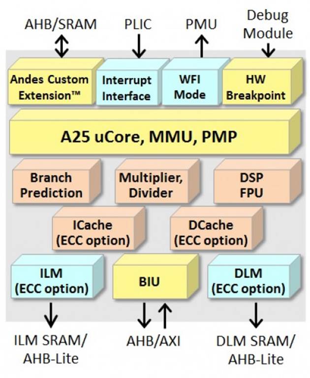
AndesCore™ A25 is a 32-bit CPU IP core based on AndeStar™ V5 architecture which incorporated RISC-V technology, it is capable of delivering high per-MHz performance and operating at high frequencies, at the same time it is small in gate count. A25 also supports single and double precision floating point and bit-manipulation instructions, and MMU for Linux based applications. A25 comes with options, including branch prediction for efficient branch execution, Instruction and Data caches, Local Memories for low-latency accesses, ECC for L1 memory soft error protection, and Andes Custom Extension™ (ACE) to add proprietary instructions to accelerate performance/power consumption critical spots.
A25’s 5-stage pipeline is optimized for high operating frequency and high performance. Features also includes PLIC and vectored interrupts for serving various types of system events, AXI 64-bit or AHB 64/32-bit bus, PowerBrake and WFI mode for low power and power management, and JTAG debug interface for development support.
Applications
- Networking and Communications
- Advanced Driver-Assistance Systems
- Video and Image Processing
- Smart wireless switch/router
- Machine/Deep Learning acceleration
Block Diagram
Development Tools
- AndeSight™ Integrated Development Environment
- COPILOT: Custom-OPtimized Instruction deveLOpment Tool for ACE
- ICE debugging hardware
Key Features and Performance
AndeStar™ V5 Architecture
| Key Features | Benefits |
|---|---|
| RISC-V RV32IMACFDBP instructions |
|
| RISC-V single and double precision floating point instruction | Accelerate the processing of high precision arithmetic |
| RISC-V bit-manipulation instructions, including the Zba, Zbb, Zbc and Zbs extensions | Benefits codes with bit-wise operations |
| Andes Extended Instructions | Andes exclusive performance and functionality enhancements |
| Andes Custom Extension™ (ACE) option to create customized instructions for software acceleration |
|
| 16/32-bit mixable instruction format | For compact code density |
| 32 general-purpose registers | For better code size and performance |
| Machine (M), User (U) and Supervisor (S) Privilege levels | For Linux and advanced operating systems with protection between kernel and user programs |
CPU Core
| Key Features | Benefits |
|---|---|
| 3.57 Coremark/MHz, 1.98 DMIPS/MHz* | Superior performance-per-MHz |
| 5-stage pipeline, with a full-cycle reserved for critical SRAM accesses | Superior performance-efficiency, while allowing for high speeds |
Extensive branch prediction features
|
|
Memory Management Unit
|
|
| Physical Memory Protection (PMP), 16 regions | Basic read/write/execute memory protection with minimum cost |
| Performance monitors | Program code performance tuning |
| StackSafe™ hardware stack protection |
|
Multiplier options
| Option to choose between speed and area according to application's requirements |
| PowerBrake technology | Performance throttling to digitally reduce power consumption |
| QuickNap™ technology | Fast power-down/wake-up support for caches |
* AndeSight v500, DMIPS/MHZ follow Dhrystone’s no-inline ground rules, best performances
Memory Subsystems
| Key Features | Benefits |
|---|---|
I-Cache & D-Cache
|
|
ILM & DLM
|
|
| Soft-error protection: ECC or parity for I-Cache and D-Cache, ILM and DLM with SRAM interface | Code and data integrity protection |
| Bus master port: AHB or AXI with 64-bit data, 32 to 64-bit address, AXI with I/D separate or joint bus | User-selectable bus interface for optimal efficiency |
| Bus save port: AHB with 64-bit data, for ILM/DLM accesses | Efficient data transfer between CPU and SoC masters |
| Core/bus clock ratio of N:1 | Simplified SoC integration |
Platform-Level Interrupt Controller (PLIC)
| Key Features | Benefits |
|---|---|
Implements RISC-V PLIC specification
| Allow individual interrupts to be serviced and prioritized without sharing |
Enhanced interrupt features
|
|
Debug Support
| Key Features | Benefits |
|---|---|
| Implements RISC-V debug specifications | Supported by industry debug tool suppliers |
| JTAG Debug Port | Industry-standard support |
| Embedded Debug Module with up to 8 triggers | Flexible configurations to tradeoff between gate count and debugging capabilities |
| Exception redirection support | Entering debugger upon selected exceptions without using breakpoints |
Performance
| Core, Process | A25 (w/o DSP, FPU), 28HPC+ | A25 (with DSP, FPU), 28HPC+ |
|---|---|---|
| Frequency (MHz) | 1000 | 1000 |
| Dynamic power (uW/MHz) | 17 | 20 |
| Area (mm2) | 0.084 | 0.165 |
* Configured with cache and MMU. SVT 9-track library, SS corner, 0.81V, -40°C, and with I/O constraint. Power consumption at TT corner, 0.9V, 25°C
Product Package
A25 with AE350 Platform
- Pre-integrated A25, PLIC, Debug Module, plus AXI/AHB Platform