AndesCore™ S8 Overview
- Secure MPU against memory tampering
- Shields against side-channel attack
- Secure debug for multi-party software development
- Flexible configurations and run-time control
Enhanced security is becoming essential as IoT devices find their way in to home automation and wearable applications. In addition to security, these applications demand low power consumption and high performance to handle compute intensive functions such as processing sensor data and wireless protocol stacks. The Andes Technology S8 processor is a new CPU core architecture based on the compute engine in the N8 core, but with added functionality to address security from hacking. The secure memory protection unit (MPU) at the center of the S8 strictly protects the execution and access according to multiple security levels. S8 also provides functions not found on competing 32-bit CPU core offerings: data and address scrambling and differential power analysis protection. The first defends against hacks that target the interface between CPU and memory. The second guards against hacking the program by observing the power use signature of the CPU.
Applications
- Smart card
- Memory card
- Health card
- Access card
- Passport
- Driving license
- Telephone card
- Library card
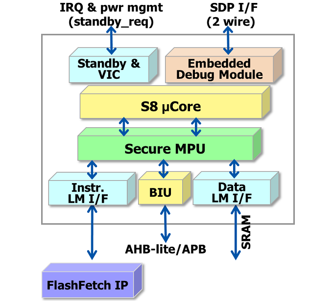
Block Diagram
Development Tools
- AndeSight™ Integrated Development Environment
- AICE JTAG/SDP debugger hardware
Key Features and Performance
AndeStar™ V3 Architecture
| Key Features | Benefits |
|---|---|
| 21st-century RISC-like instruction set | 21st-century RISC-like instruction set |
| V3 subset for MCU most frequency used instructions | Smaller die size and lower power consumption |
| 16/32-bit mixable opcode format | Smaller code size |
| AndeStar Security Extension Micro Profile | Secure core capabilities |
| All-C Embedded Programming | Faster SW development and easier maintenance |
| Hardware divider | More performance |
| Direct support of up to 32 interrupts with programmable priority levels | Quick identification of interrupt sources and fast assignment of service routines |
| 16MB or 4G address space | Less address bits option leading to small gate count |
| Memory mapped IO | Easy to program and friendly to compiler |
CPU Core
| Key Features | Benefits |
|---|---|
| 1.53 DMIPS/MHz* 3.02 CoreMark/MHz* | Superior performance-per-MHz |
| 3-stage pipeline | Superior performance-efficiency, while allowing for high speeds |
| Secure MPU & secure debugging | Code and data protection |
Choice of multipliers
| Application specific configurations
|
| Processor state bus | Simplification SoC design and debugging |
| Performance monitors | Program code performance tuning |
Interface to FlashFetch IP (Separately licensable) which contains following options
| Slow flash memory acceleration and power consumption reduction |
| Extensive clock gating and logic gating | Lower power |
| N:1 core/bus clock ratios | Simplified SoC integration |
| Low-latency vectored interrupt | Faster context switch for real-time applications |
| Completion of most operations in 1 cycle Single-cycle capable for Local Memory and AHB bus accesses | Better performance-efficiency |
* BSP v4.2.0, DMIPS/MHZ without no-inline option, best performances
Memory Subsystems
| Key Features | Benefits |
|---|---|
Optional External Instruction and Data Local Memory
| Higher efficiency for program execution
|
| BIU supports AHB-lite or APB | User-selectable bus interface for optimal efficiency |
Debug Support
| Key Features | Benefits |
|---|---|
| 2-wire Serial Debug Port or 5-wire JTAG Debug Port | Low-cost 2 wire support and industry-standard 5-wire support |
Embedded Debug Module (EDM)
|
|
Performance
| Process | 28HPM |
|---|---|
| Frequency (MHz) | 780 |
| Dynamic power (uW/MHz) | 8.0 |
| Area (mm2) | 0.024 |
* Base configuration, LVT library; Frequency at slow process corner, 0.81V, 125°C and without I/O constraint; Power consumption at typical process corner, 0.9V, 25°C