AndesCore™ N7 Overview
- Seamless migration to full 32-bit environment from 8/16-bit MCUs
- Low power consumption for extended battery life
- Small footprint with low gate count and high code density
- Speed-up and power reduction for Flash accesses by FlashFetch technology
The AndesCore™ N7, a family of small cores serves applications including embedded processing devices that require low energy consumption, such as controllers for touch screen, storage, hand-held devices, sensors, and for network connectivity applications like loT (Internet-of-Things). The N7’s ultra-low power consumption and small size was created for performance constrained SOC designs. The N7’s features the latest AndeStar™ V3m architecture and a 2-stage pipeline that helps delivering an impressive 168 DMIPS/mW, >40% better than competitive products. Its FlashFetch technology can boosts higher latency flash memory performance without consuming added power. The AndesCore™ N7 can be as small as 12K gates. This makes it an ideal alternative to 8051 and other 8-bit processor cores, while delivering the programmability benefits of a 32-bit processor solution.
Applications
- Internet of Things (IOT)
- Sensor fusion
- Smart energy monitor and control
- Home security and remote control
- Gas/water/electronic metering
- Medical device
- Wearable device
- Education device
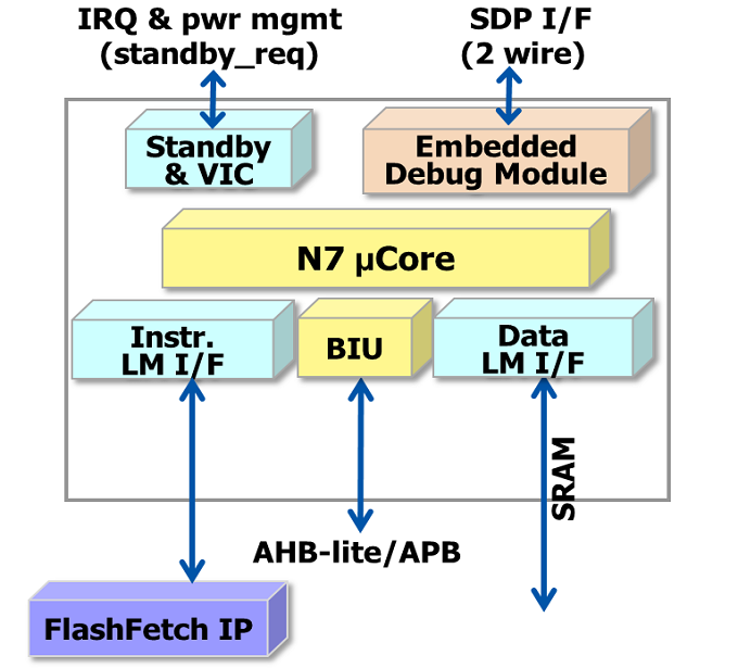
Block Diagram
Development Tools
- AndeSight™ Integrated Development Environment
- AICE JTAG/SDP debugger hardware
Key Features and Performance
AndeStar™ V3 Architecture
| Key Features | Benefits |
|---|---|
| 21st-century RISC-like instruction set | Better performance for modern compiler |
| V3 subset for MCU most frequency used instructions | Smaller die size and lower power consumption |
| 16/32-bit mixable opcode format | Smaller code size |
| All-C Embedded Programming | Faster SW development and easier maintenance |
| Hardware divider | More performance |
| Direct support of up to 32 interrupts with programmable priority levels | Quick identification of interrupt sources and fast assignment of service routines |
| 16MB/4G address space | Less address bits option leading to small gate count |
| Memory mapped IO | Easy to program and friendly to compiler |
CPU Core
| Key Features | Benefits |
|---|---|
| 1.71 DMIPS/MHz* 3.36 CoreMark/MHz* | Superior performance-per-MHz |
| 2-stage pipeline | Superior performance-efficiency, while allowing for high speeds |
Choice of multipliers
|
|
| Hardware stack protection | Stack size determination and runtime overflow error detection |
| Processor state bus | Simplification SoC design and debugging |
| Performance monitors | Program code performance tuning |
Interface to FlashFetch IP (separately licensable) which contains following options
| Slow flash memory acceleration and power consumption reduction |
| Extensive clock gating and logic gating | Lower power |
| N:1 core/bus clock ratios | Simplified SoC integration |
| Low-latency vectored interrupt | Faster context switch for real-time applications |
| Completion of most operations in 1 cycle Single-cycle capable for Local Memory and AHB bus accesses | Better performance-efficiency |
| PowerBrake technology | Peak power consumption reduction |
* BSP v4.2.0, DMIPS/MHZ without no-inline option, best performances
Memory Subsystems
| Key Features | Benefits |
|---|---|
Optional External Instruction and Data Local Memory
| Higher efficiency for program execution
|
| BIU supports AHB-lite or APB | User-selectable bus interface for optimal efficiency |
Debug Support
| Key Features | Benefits |
|---|---|
| 2-wire Serial Debug Port or 5-wire JTAG Debug Port | Low-cost 2 wire support and industry-standard 5-wire support |
Embedded Debug Module (EDM)
|
|
Performance
| Process | 90LP | 40LP | 28HPM |
|---|---|---|---|
| Frequency (MHz) | 50 | 50 | 50 |
| Dynamic power (uW/MHz) | 8.7 | 3.9 | 2.1 |
| Area (mm2) | 0.04 | 0.015 | 0.007 |
* Base configuration, Power consumption at typical process corner, Vdd (90LP: 1.2V, 40LP: 1.1V, 28HPM: 0.9V), 25°C
| Process | 40LP | 28HPM |
|---|---|---|
| Frequency (MHz) | 279 | 506 |
| Dynamic power (uW/MHz) | 5.9 | 3.9 |
| Area (mm2) | 0.026 | 0.013 |
* Base configuration, LVT library; Frequency at slow process corner, 40LP:0.99V, 28HPM:0.81V, 125°C and without I/O constraint; Power consumption at typical process corner, Vdd (40LP: 1.1V, 28HPM: 0.9V), 25°C
