AndesCore™ N9 Overview
- High performance V3 ISA on a compact CPU architecture
- Superior total performance deliverable
- Efficient pipeline optimized for Local Memory accesses
- High configurability including AXI bus support
The AndesCore N9 Family is intended for deeply embedded applications that require optimal interrupt response features, including wireless networking and sensors, microcontrollers, automotive electronics, and industrial control systems. The low-power N9 Family of processors features low gate count, low interrupt latency, and low-cost debug. The processor family provides superior performance and excellent interrupt handling response while meeting the challenges of low dynamic and static power constraints.
The AndesCore N9 Family of CPU cores implement v3, the AndeStar™ patented 32-bit RISC-style CPU architecture. The designer can configure certain parameters to adjust the CPU’s size, power, and performance. For example, the N9 core can be configured with 16 or 32 general registers, two or three read ports on the register file, one or two write ports, a fast or a small multiplier, a 24-bit or 32-bit address space, and different bus (APB, AHB, AHB-Lite, AXI) interfaces to connect to the rest of the system.
Applications
- Wireless device
- Wireless charger
- Touch screen controller
- Storage device
- Industrial control
- Biometrics device
- GPS
- Game console
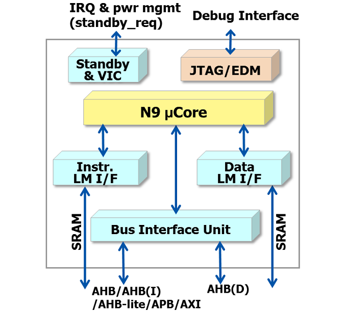
Block Diagram
Development Tools
- AndeSight™ Integrated Development Environment
- AICE JTAG/SDP debugger hardware
Key Features and Performance
AndeStar™ V3 Architecture
| Key Features | Benefits |
|---|---|
| 21st-century RISC-like instruction set | Better performance for modern compiler |
| 16/32-bit mixable opcode format | Smaller code size |
| Optional saturation instructions | Efficient voice applications |
| 16 or 32 general-purpose registers | Trade-off between core size and performance requirements |
| All-C Embedded Programming | Faster SW development and easier maintenance |
| Shadow stack pointer | Efficiency and protection with a dedicated kernel stack pointer |
| Aligned and unaligned load/store multiple word instructions and post-increment load/store memory accesses | Better program code size and performance |
| Direct support of up to 64 interrupts with programmable priority levels | Quick identification of interrupt sources and fast assignment of service routines |
| 4G or 16MB address space | Full range or less address bits leading to small gate count |
| Memory mapped IO | Easy to program and friendly to compiler |
CPU Core
| Key Features | Benefits |
|---|---|
| 2.21 DMIPS/MHz* 3.59 CoreMark/MHz* | Superior performance-per-MHz |
| 5-stage pipeline | Superior performance-efficiency, while allowing for high speeds |
| Static branch predication | Better performance for branches |
| Hardware stack protection | Stack size determination and runtime overflow error detection |
| Processor state bus | Simplification SoC design and debugging |
| Performance monitors | Program code performance tuning |
Choice of multipliers
| Application specific configurations
|
| Fast multipliers (1 cycle) | More performance |
| Extensive clock gating and logic gating | Lower power |
| N:1 core/bus clock ratios | Simplified SoC integration |
| Low-latency vectored interrupt | Faster context switch for real-time applications |
| Completion of most operations in 1 cycle Single-cycle capable for Local Memory and AHB bus accesses | Better performance-efficiency |
| PowerBrake technology | Peak power consumption reduction |
* BSP v4.2.0, DMIPS/MHZ without no-inline option, best performances
Memory Subsystems
| Key Features | Benefits |
|---|---|
Optional External Instruction and Data Local Memory
| Higher efficiency for program execution
|
| BIU supports 32-bit AHB/2AHB/AHB-lite/APB/AXI | User-selectable bus interface for optimal efficiency |
Debug Support
| Key Features | Benefits |
|---|---|
| 2-wire Serial Debug Port or 5-wire JTAG Debug Port | Low-cost 2 wire support and industry-standard 5-wire support |
Embedded Debug Module (EDM)
|
|
Performance
| Process | 90LP | 40LP | 28HPM |
|---|---|---|---|
| Frequency (MHz) | 50 | 50 | 50 |
| Dynamic power (uW/MHz) | 25.9 | 10.6 | 6.2 |
| Area (mm2) | 0.10 | 0.035 | 0.018 |
* Base configuration, RVT library. ; Power consumption at typical process corner, Vdd (90LP: 1.2V, 40LP:1.1V, 28HPM: 0.9V), 25°C
| Process | 40LP | 28HPM |
|---|---|---|
| Frequency (MHz) | 632 | 950 |
| Dynamic power (uW/MHz) | 11.1 | 6.8 |
| Area (mm2) | 0.062 | 0.027 |
* Base configuration, LVT library; Frequency at slow process corner, 40LP: 0.99V, 28HPM:0.81V, 125°C and without I/O constraint; Power consumption at typical process corner, Vdd (40LP:1.1V, 28HPM: 0.9V), 25°C
